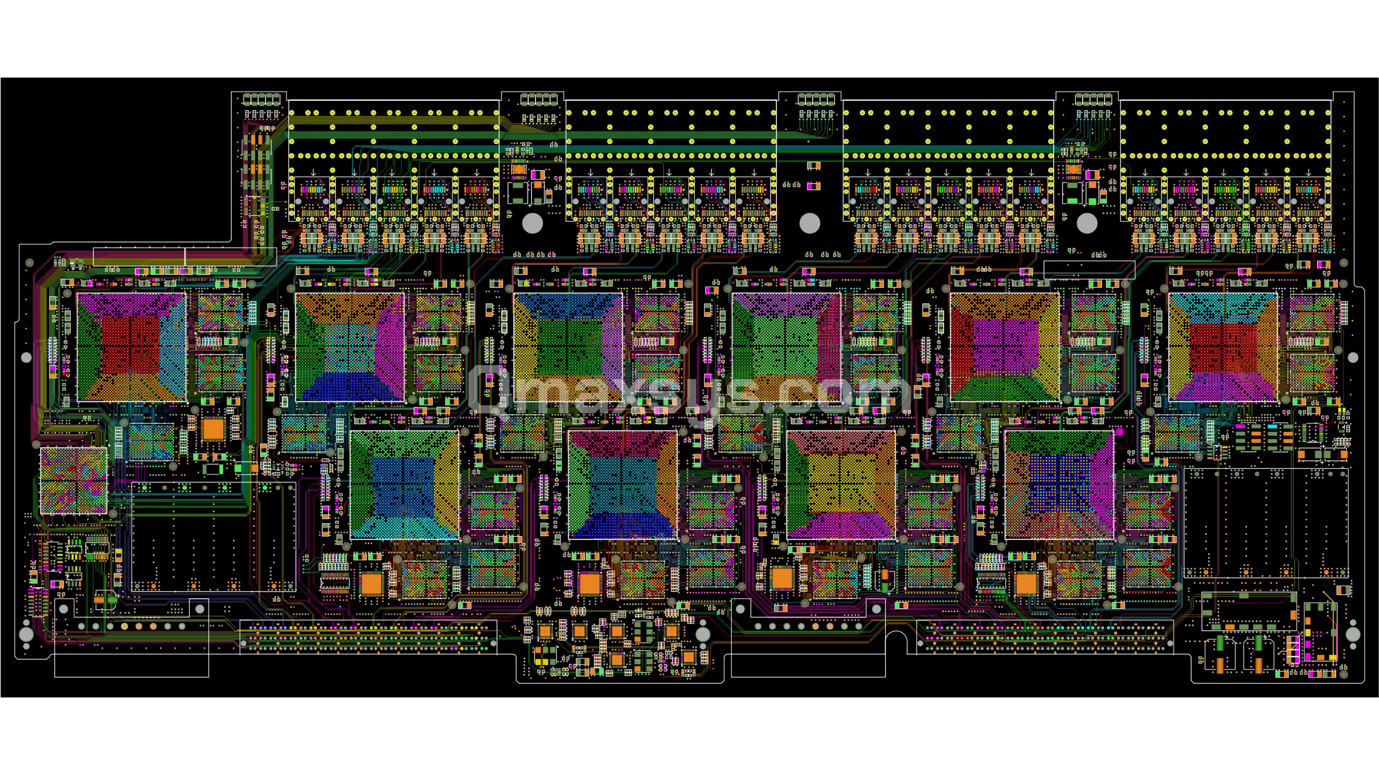
40-Port 10GbE Core-Router Line Card
Project Overview
Qmax Systems was engaged to execute the full physical PCB design of a high-density 40-port 10 Gigabit Ethernet line card for a modular core switch/router chassis. The customer supplied verified schematics and a complete design-input package; Qmax owned the layout of a 24-layer, controlled-impedance, carrier-grade line card carrying 400 GbE of aggregate line-side capacity into the chassis switch fabric. With over 36,000 pins, a very large high-speed SRAM subsystem, and 40 optical ports to route on a single card, high-speed signal integrity, memory-interface timing, and manufacturability were the central engineering challenges. Qmax delivered a fabrication-ready design closing on SI, PI, and DFM targets without a re-spin.
Application Brief
The board is a front-line traffic-ingress line card for a modular, chassis-based core switch/router used by service providers and large enterprises for high-capacity Ethernet aggregation and routing. It presents 40 × 10 Gigabit Ethernet SFP+ optical ports on the front panel — 400 GbE of aggregate line-side capacity — driven by ten Cortina Systems CS3487 multi-port 10GbE devices, and connects to the chassis switch-fabric cards through high-speed backplane fabric connectors. Line-rate packet framing, classification, and forwarding are backed by a large JEDEC-standard QDR-II SRAM subsystem for packet buffering and lookup tables, with low-jitter LVPECL clock distribution feeding the high-speed serial interfaces. At the PCB level this translates into dense high-speed serial routing for 40 optical ports, an extensive memory-interface routing problem, and full hot-swap power and manageability support on a single controlled-impedance card.
Qmax Scope
Qmax Systems owned the full PCB design of the line card, from design-input review through fabrication data release:
- Design-input review — captured customer schematics, mechanical outline, BoM, net classes, and electrical constraints across high-speed serial, memory, analog, and power domains
- 24-layer stackup design — defined a controlled-impedance stackup with 10 routing layers and 10 power/ground planes for a very high pin- and via-density board
- 40-port optical routing — floor-planned and routed the 40 × 10GbE SFP+ front-panel ports with matched high-speed serial (XAUI-class) attachment to the ten Cortina CS3487 port devices
- High-speed SRAM subsystem — routed a large high-speed SRAM memory array (packet-buffer / lookup) with length- and skew-matched data, address, and control buses
- Backplane fabric escape — designed the high-speed backplane fabric connector escape carrying line-card traffic to the chassis switch fabric
- Power delivery network design — planned a multi-rail PDN (12 V main through 3V3 / 2V5 / 1V8 / 1V2) with margining, sequencing, and power-good supervision for hot-swap operation
- Signal integrity review — impedance, insertion/return-loss, crosstalk, and skew verification for the optical-port serial links and memory interfaces
- Power integrity review — PDN impedance targeting and decoupling strategy across the plane structure feeding the high pin-count logic and QDR-II SRAM array
- High-density via planning — managed nearly 25,000 through-vias with disciplined via-field and antipad strategy to keep routing channels open on a 24-layer board
- DFM and fabrication release — DFM review against fab and assembly constraints, drill/padstack audit, and full Gerber / fabrication data package release
Challenges & Resolutions
Routing 40 Optical Ports on One Card
The 40 × 10GbE SFP+ ports and their high-speed serial attachment were floor-planned in port banks with matched-length, reference-continuous routing to preserve eye margin across every port.
36,000+ Pins on 24 Layers
An exceptionally high pin and net density was resolved through careful device placement, layer-pair assignment, and via-field discipline to fit all routing within the layer budget.
Large High-Speed SRAM Timing
The multi-device SRAM array's data, address, and control buses were length- and skew-matched with matched terminations to close read/write timing at line rate.
Backplane Fabric Integrity
High-speed serial links to the chassis fabric connectors were routed with controlled impedance and matched skew to sustain signal integrity across the backplane.
Front-Panel Optical Density
The SFP+ cage banks were placed and escaped to balance thermal, mechanical, and high-speed routing constraints along the front edge.
Low-Jitter Clock Distribution
Multiple low-jitter LVPECL reference clocks were distributed to the high-speed serial interfaces with guarding and matched lengths, isolated from noisy regions.
Multi-Rail Hot-Swap Power
The sequenced, margined multi-rail PDN with power-good supervision was laid out with wide, low-impedance copper for reliable live insertion/removal.
Mixed-Signal Isolation
Analog supply and sensing nets were partitioned from digital switching and high-current regions to protect the sensitive serial and memory interfaces.
Carrier-Grade DFM Closure
The layout was reviewed against fabrication and EMS constraints (drill sizes, aspect ratio, connector press-fit, padstacks) to release manufacturing data without a re-spin.
Major HW Components
Cortina Systems CS3487 (×10)
Multi-port 10GbE MAC/PHY-class devices providing the port interface across the 40-port array (four 10GbE ports per device)
QDR-II High-Speed SRAM (30 Devices)
Large JEDEC-standard QDR-II SRAM array (2M×36 devices) for packet buffering and forwarding/lookup tables
ON Semiconductor NB4L7210 (×5)
1:10 LVPECL/LVDS clock fanout buffers distributing low-jitter references to the high-speed serial interfaces
40 × SFP+ Optical Cages
Major Interfaces
40 × 10GbE Optical Ports
Front-panel SFP+ optical ports delivering 400 GbE of aggregate line-side capacity
High-Speed Serial Attach (XAUI-Class)
Matched multi-lane serial links between the SFP+ optical ports and the Cortina CS3487 port devices
Backplane Switch-Fabric Links
High-speed serial connections via 144-pin backplane connectors into the chassis switch fabric
QDR-II SRAM Buses
Matched data, address, and control buses to the 30-device QDR-II SRAM array, with LTC3413 bus termination
Thermal Monitoring
Temperature-sensor interfaces for line-card health and fan/thermal control
Multi-Rail DC Power
12 V main input with 3V3 / 2V5 / 1V8 / 1V2 derived rails for the processing, memory, and optical subsystems
PCB Design Specifications
Summary
Qmax Systems delivered a complete, fabrication-ready layout of a 24-layer, 40-port 10 Gigabit Ethernet core-router line card carrying 400 GbE of aggregate line-side capacity. Despite fewer layers than a comparable fabric card, this was the highest-density board of its platform — over 36,000 pins, and a large high-speed SRAM subsystem packed onto a single controlled-impedance card. The design closed on signal integrity, power integrity, and DFM targets from customer design inputs through to Gerber release, demonstrating Qmax's capability to route the most pin- and via-dense high-speed boards to manufacturing without a re-spin.