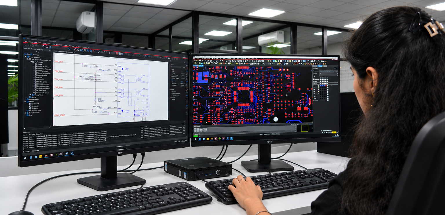
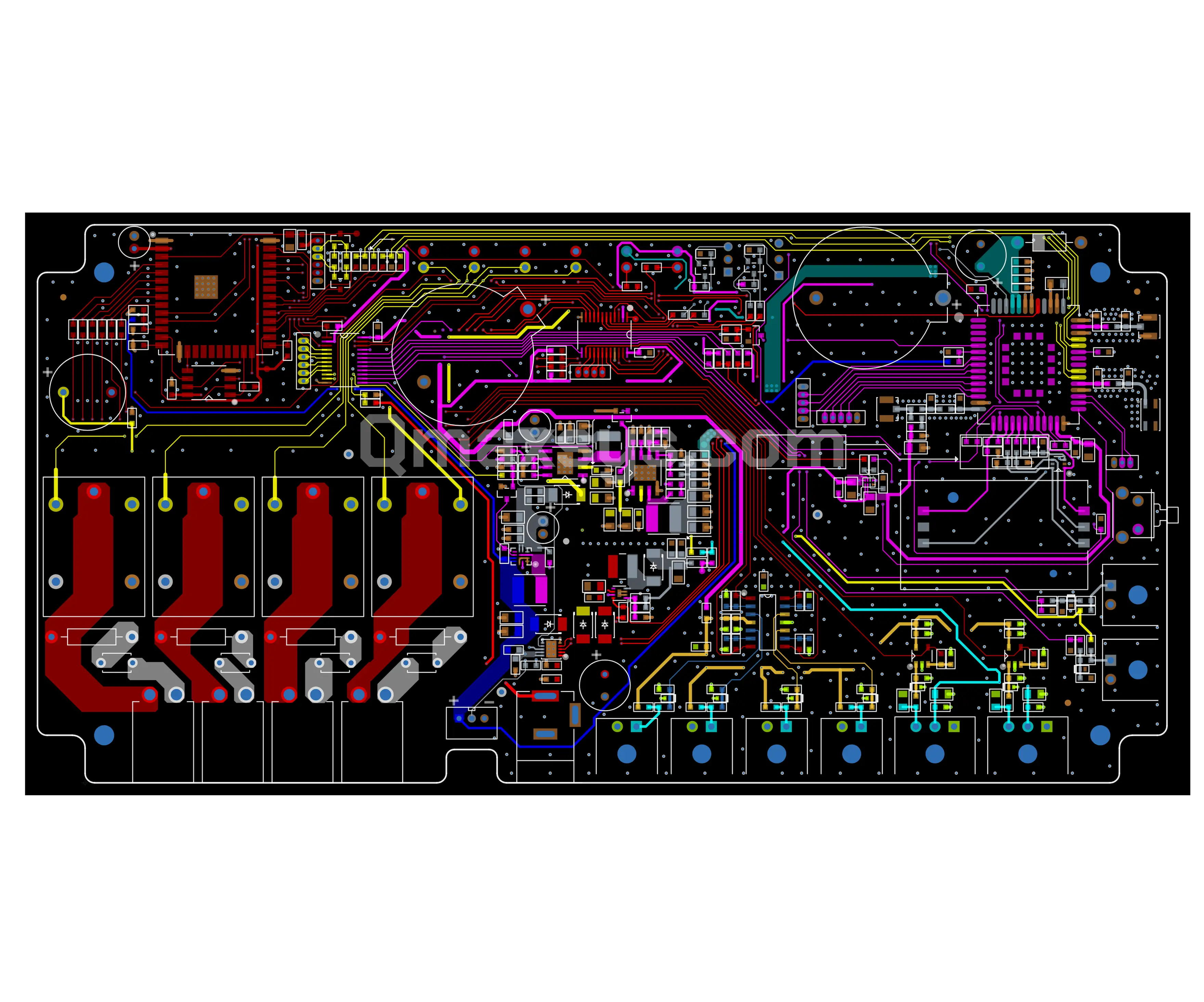
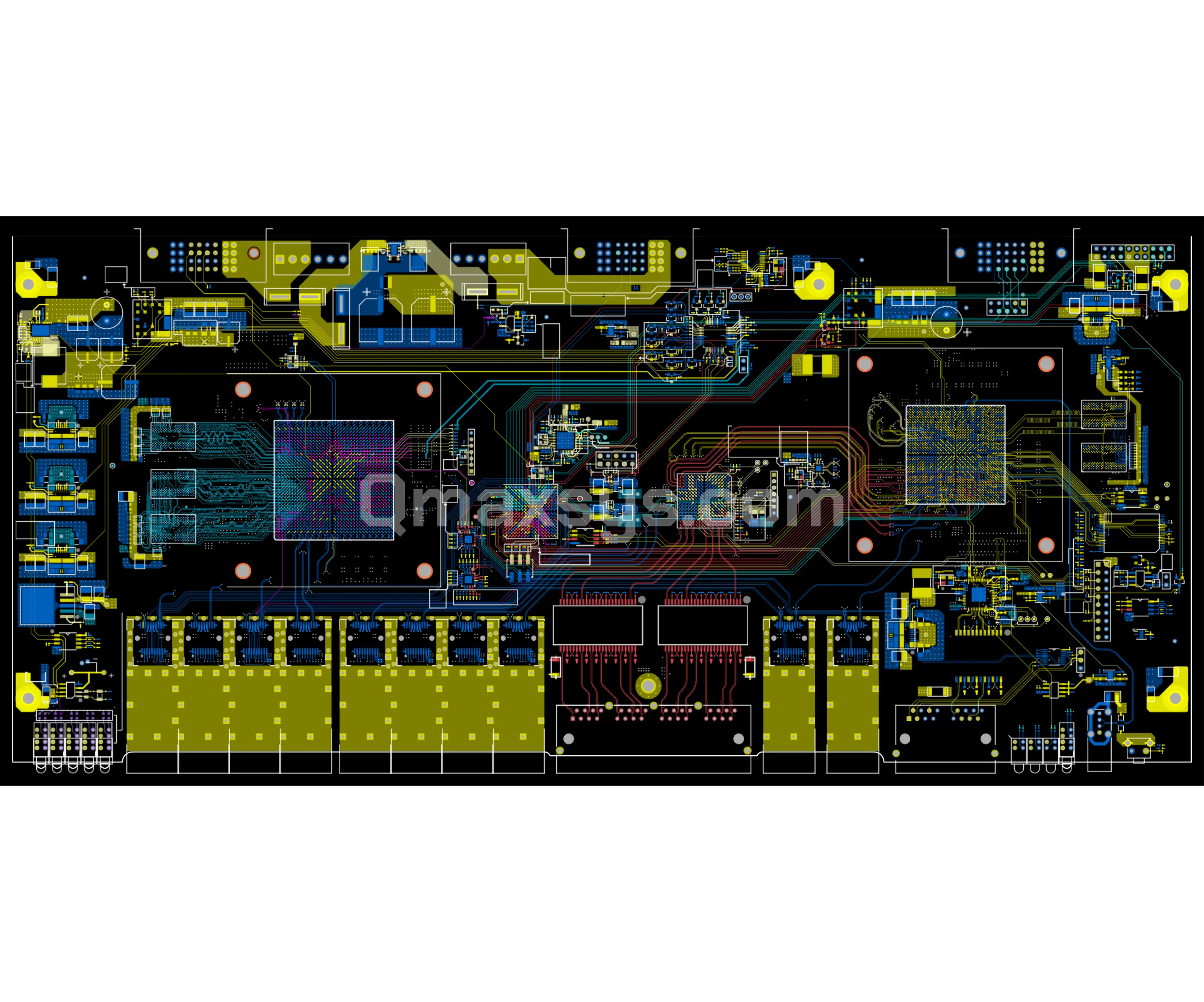
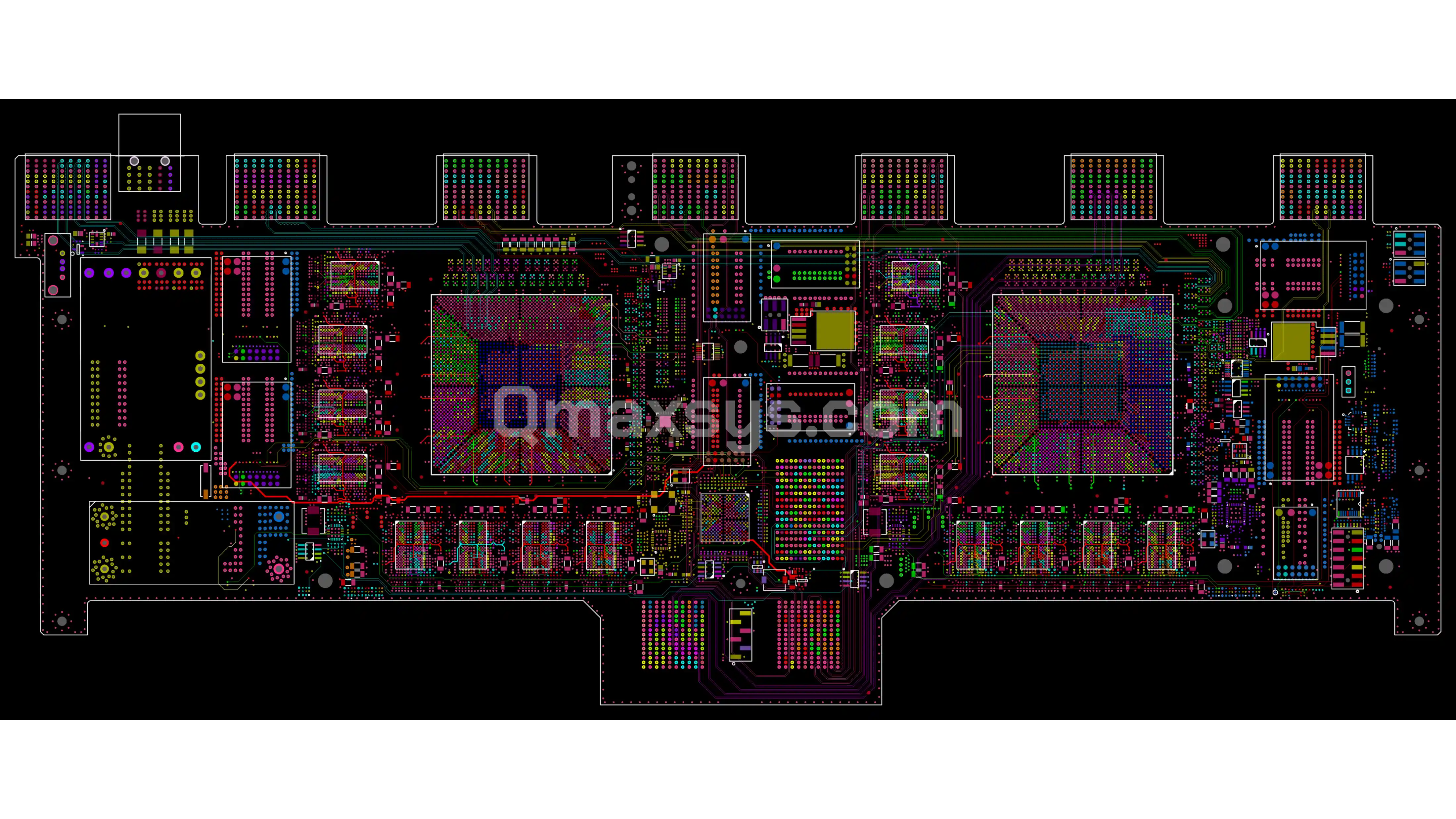
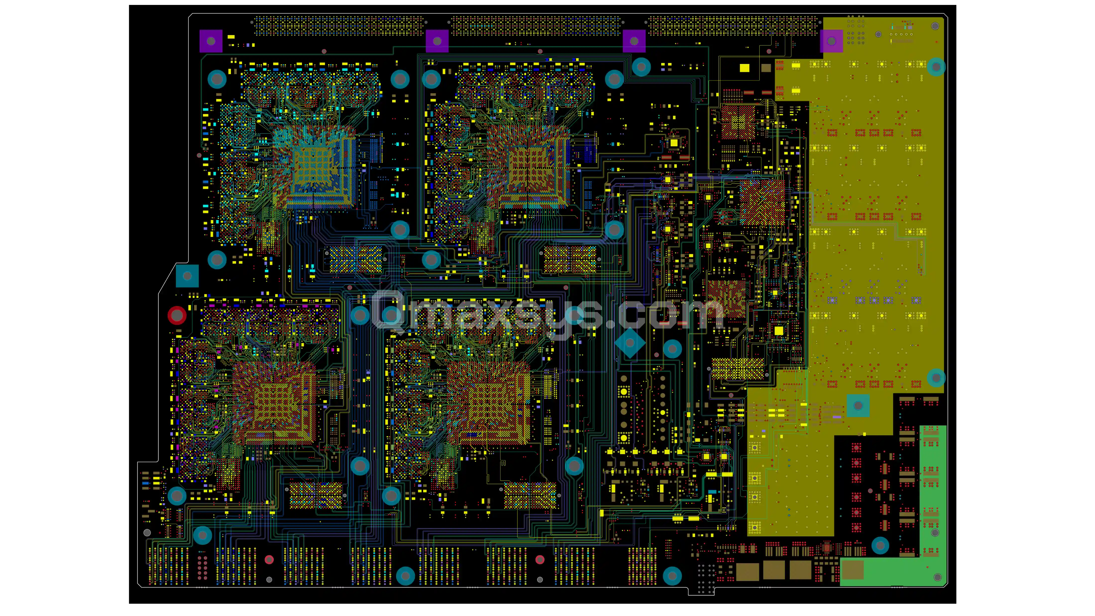
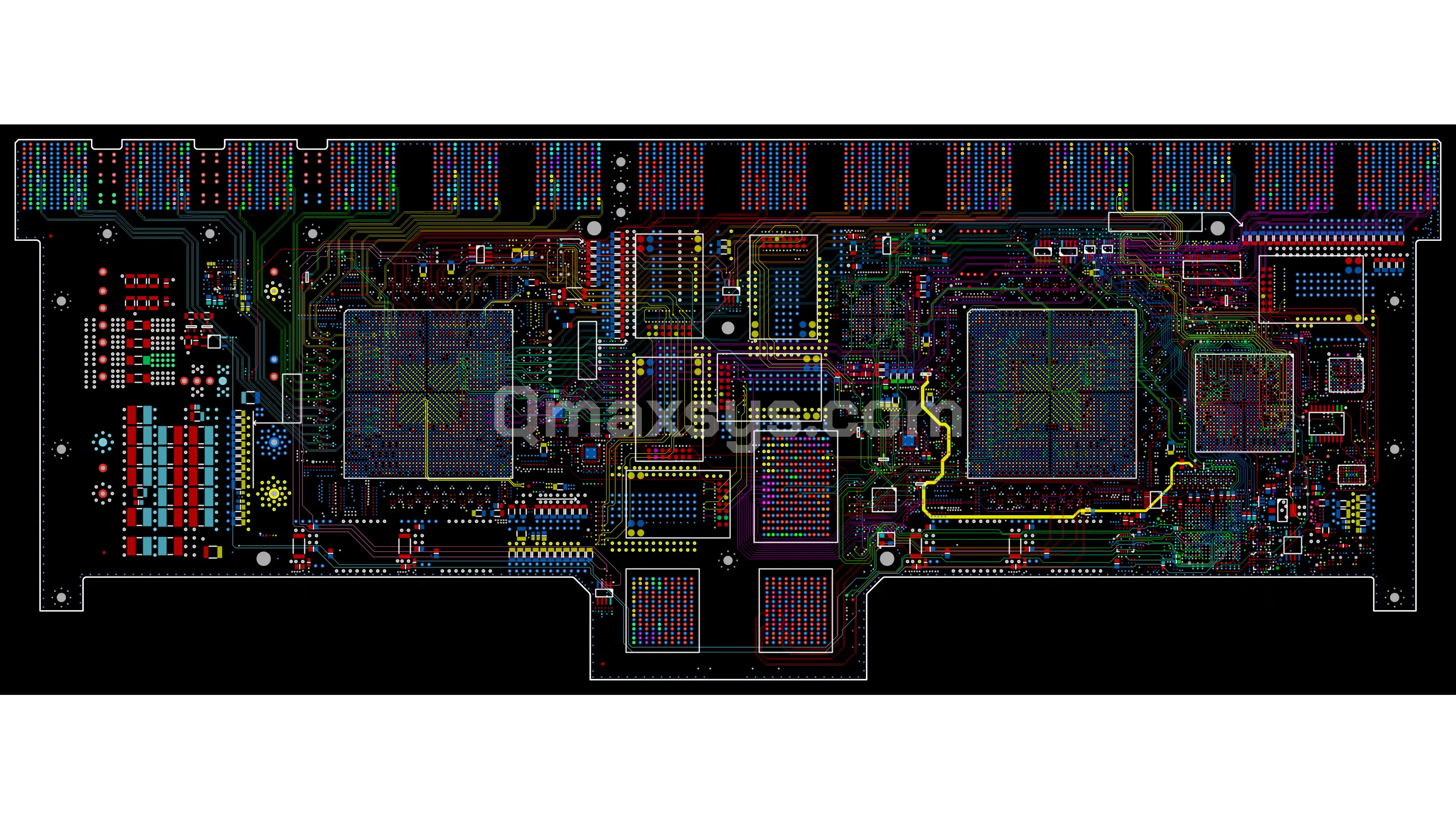
Qmax Systems has laid out analog and mixed-signal boards since 1997 — 29 years of domain partitioning, grounding architecture, guarding and shielding, precision placement, converter and reference layout, and characterization against a measured noise target. Every PCB designer on the team is an Electrical or Electronics Engineer who can read the circuit and run the noise analysis, and the team holds IPC CID certification. Several have close to forty years at the board.
In analog design the layout is the circuit. A schematic that is electrically perfect will still measure badly if digital return current crosses the analog reference, if a high-impedance node sits three millimeters from a switching node, if the reference is routed as though it were a supply, or if a matched pair straddles a thermal gradient. None of those faults appear in simulation of the schematic. All of them are decided by where copper goes.
The working method is to remove the coupling mechanism rather than filter its result. Delivered boards include a 32-channel simultaneous-sampling acquisition board measured at 90 dB SNR, five metering channels holding roughly 1% accuracy on a board pressed against thirty switching mains relays, and femtofarad-level capacitance measurement through wiring whose own parasitic capacitance was orders of magnitude larger than the signal.
Isolated LDO-filtered analog rails, references treated as signals
Verification & Release
DRC and ERC, DFM, DFA and DFT review, Gerber or IPC-2581 package
Analog and Mixed-Signal Boards We Design
Precision Data Acquisition Boards
Multi-channel boards where channels must be sampled simultaneously and matched to each other, not merely digitized accurately one at a time. Channel-to-channel skew and gain matching are the specifications that get overlooked, and they are decided by placement symmetry.
Simultaneous-sampling SAR arrays to 32 channels on one board
Convert-start and clock distribution matched across every converter
Separate analog and digital supply domains with controlled crossings
Input protection and TVS clamping on every channel
Sensor Front-End and Instrumentation Boards
Boards where the sensor output is small, high-impedance, or both, and where the layout has to present that impedance without loading it or contaminating it. Guarding matters more here than filtering.
Bridge, strain gauge, load cell, thermocouple and RTD front-ends
Transimpedance layout for photodiodes and other current-output sensors
Femtofarad-class capacitance and impedance measurement
Electrochemical impedance spectroscopy front-ends
Medical and Bio-Signal Boards
Patient-connected boards where microvolt bio-potentials coexist with digital processing, and where the isolation barrier is a layout geometry problem as much as a component selection problem. Designed inside an ISO 13485 quality system.
ECG, PPG, GSR and bio-impedance front-end layout
MEMS acoustic and bio-acoustic signal chains
Patient-side isolation with creepage and clearance per IEC 60601-1 and IPC-2221
Leakage-current-aware routing and barrier keep-outs
Measurement Inside High-Power Environments
Boards where the measurement is placed deliberately next to the thing generating the noise, because that is where the current and voltage have to be sensed. This is the hardest class of mixed-signal layout and the one Qmax is asked for most.
Boards where a precision analog section shares copper with an applications processor, a radio or a switching regulator. The partition boundary and the crossing discipline are what make the coexistence work.
Analog front-ends partitioned from Arm SoC and MCU digital sections
Radio sections isolated from measurement paths on the same board
Converter-to-processor interfaces on SPI, LVDS and parallel buses
Sampling clock domains kept separate from digital switching
Low-Power and Battery-Operated Boards
Boards where the analog front-end has to stay accurate at a quiescent current that leaves the product a useful run time, and where power-domain partitioning is a layout decision rather than a firmware one.
Nanoampere-class front-end layout with leakage-aware routing
Power-domain partitioning for shutdown and fast clean wake
Coin-cell and single-cell Li-ion boards with brown-out margin
Two-layer designs where cost and size are the binding constraints
Board Complexity We Design To
Parameter
What we design to
Boards we have designed
Layer count
2 to 36 layers available; precision work usually lands between 2 and 8
8 layers on a 32-channel acquisition board measured at 90 dB SNR, and 2 layers on a railway controller carrying two radios and relay drive
Routing and plane budget
Assigned for reference continuity under the converters before routing space is considered
4 routing over 4 plane on the acquisition board — half the stack-up spent on references, deliberately
Trace and space
Standard geometry is normally sufficient; fine geometry is specified only where it earns something
Rarely the binding constraint on precision analog boards — partitioning and placement decide the measurement
Drill and via structures
Through-hole where it suffices, blind and buried only where the escape genuinely demands it
1,619 through-vias and no microvia structures on the acquisition board — through-hole was sufficient and cheaper, which is the right answer when nothing needs more
Isolation and barriers
Creepage and clearance from IEC 60601-1 where patient-connected, cross-checked against IPC-2221
Galvanic isolation between a metering domain and its processor across a mains barrier, with high-integrity signaling across it
Board thickness
Chosen for the reference structure and the mechanical envelope
68.8 mils on the acquisition board and 63 mils on a metering board, both read from the design database
Controlled impedance
Applied to converter interfaces and clock distribution, not blanket-applied across the board
Converter and clock paths held to target; the rest of the board left free so partitioning was not compromised by an unnecessary constraint
Channel count and matching
Simultaneous-sampling arrays with matched convert-start and clock distribution
32 channels of 16-bit at 30 kSPS measured at 90 dB SNR, on four independent SPI buses with twenty convert-start nets
Measurement extremes
From femtofarad-class capacitance and microampere sensing to metering beside switching mains
Femtofarad-level capacitance resolved through wiring with far larger parasitic capacitance; ~1% metering accuracy against thirty switching mains relays
Base materials
FR-4 where suitable per IPC-4101; low-loss laminate where dielectric absorption would cause settling error
FR-4 on most precision work. Low-loss specified only where a high-impedance node or a high-frequency subsystem justified the cost
Performance class
IPC-6012 Class 2 or Class 3, with Class 3 normal on medical and instrumentation builds
Class 3 specified on medical and instrumentation builds where the performance class requires it
Applications & Real-World Project Experience
Mixed-signal PCB layout for a cold-storage IoT monitoring board, partitioning the ESP32 digital and radio sections from the analog sensor chain - four NTC temperature inputs, dual pressure interfaces, and 12-/16-bit ADC acquisition - with dedicated ground references for low-noise capture.
High-density mixed-signal layout for a 240-channel industrial I/O controller, isolating the pressure-sensor analog front end and delta-sigma ADC from high-side digital switching across a 6-layer, 2,600+ component board.
EMI-conscious 2-layer mixed-signal layout for a railway-grade lubrication controller, partitioning BLE/GSM RF, sensor inputs, and relay drive circuits with surge-hardened field I/O for track-side deployment.
Partition the Return Current, Not Just the Components
The first layout decision on a mixed-signal board is not where parts go but where return current is allowed to flow. Domains are assigned before placement, the reference is deliberately partitioned, and every crossing is a single known bridge — so return current has one path and that path is a design choice rather than an accident of routing.
Analog, digital and power zones assigned before any part is placed
Moat-and-bridge partitioning with one controlled crossing per domain pair
Reference continuity checked at every plane transition
No digital routing permitted across an analog partition, enforced as a rule
On two-layer boards, every return path drawn explicitly rather than assumed
Guard the High-Impedance Node
When a high-impedance input sits near a fast-switching node, geometry beats filtering every time. Copper between them, a guard held at the signal's own potential, and physical distance are all cheaper and more effective than any component added later — and on a femtofarad measurement they are the only thing that works at all.
Guard rings and driven guards around high-impedance and picofarad-class nodes
Faraday shields and shield-can provision over sensitive front-end sections
Grounded copper placed deliberately between aggressor and victim
Spacing to IPC-2221, with leakage-aware routing on electrometer-class inputs
Solder-mask and surface-finish choices considered where surface leakage matters
Place for Symmetry and Thermal Quiet
Matched components only stay matched if they see the same environment. A matched pair straddling a thermal gradient drifts differentially, a reference next to a dissipating regulator moves with load, and two channels of a supposedly identical array measure differently because one sits closer to the processor.
Matched and differential pairs placed symmetrically, not merely adjacently
Precision references given their own placement, routing and thermal separation
Channel-to-channel symmetry enforced across multi-channel arrays
Isolated LDO-filtered analog rails routed away from switching domains
Sampling clock kept in its own domain, because jitter converts to amplitude error
Coupling mechanism
How it reaches the signal
What the layout does about it
Ground return coupling
Return current from a digital or power load crossing the analog reference
Deliberate plane partition with a single bridge, so the return has one known route rather than whichever way is shortest
Conducted supply noise
Switching ripple on a shared rail reaching the front-end supply pin
Separate quiet rail, isolated LDO post-regulation, local decoupling sized to the spectrum rather than by habit
Capacitive coupling
dV/dt on a switching node displacing charge into a high-impedance input
Physical separation, grounded copper between the two, guard rings and driven guards at signal potential
Inductive coupling
di/dt in a current loop linking flux into the signal loop
Both loop areas minimized, loops oriented orthogonally, differential pairs routed tight, switching loop shrunk at source
Common-mode injection
Common-mode current through the input pair or across an isolation barrier
Balanced differential routing with matched impedance to ground, barrier keep-outs, low-capacitance isolator placement
Thermal and drift error
Gradients across a matched pair, self-heating, dissimilar-metal junctions
Symmetric placement, thermal separation from dissipating parts, zero-drift devices given quiet copper
Sampling clock jitter
Phase noise on the converter clock converting directly into amplitude error
Clock in its own domain with a controlled-impedance route, reference separated from digital switching
Surface and dielectric leakage
Contamination or dielectric absorption at very high impedance nodes
Guarding, mask and finish selection, and low-dielectric-absorption laminate where the impedance justifies it
How a Precision Board Gets From Netlist to Release
The Errors Here Are Invisible Until They Are Measured
A high-speed board fails loudly — the link will not train. A precision board fails quietly: it works, and reads three millivolts off, and nobody knows why for a month. That is why Qmax runs in-house scripts that audit the database between stages for the specific faults a standard DRC cannot express — a partition crossed by a net nobody flagged, an analog rail sharing a return with a switching load, a guard ring left unconnected.
Stage-gate checklists, each with a named owner and a recorded outcome
In-house scripts that audit domain crossings, reference continuity and guard connectivity
Each check cites the document it enforces — IPC-2221 for spacing and generic design, IPC-6012 for performance class, IPC-A-600 for board acceptability, IPC-A-610 with J-STD-001 for assembly, IPC-2231 for design-for-excellence — so a finding is arguable against a standard rather than against an opinion
Release Is Read Aloud by Two People
One engineer reads the item, a second confirms the state out loud. It sounds like a flight crew running a pre-flight checklist, and that is deliberate. On a precision board the item most often skipped by a solo reviewer is the one that looks obviously fine — the single bridge across the moat, the reference tie nobody wants to question at release.
Challenge and response on every release item, spoken and confirmed
Every partition crossing named, justified and confirmed aloud
Every high-impedance node confirmed guarded; every reference traced to its single point
Sign-off recorded against a name, not just a date
What Lands in Your Hands
A release package complete enough that the fabrication partner needs to ask nothing, with the analog-specific requirements written on the drawing rather than left as folklore. You own all of it.
Gerber and drill data, or IPC-2581 (DPMX) and ODB++
Fabrication drawing with stack-up, impedance table where applicable, and material call-outs
Assembly drawing with shield-can, guard and keep-out requirements marked
BoM, netlist and IPC-D-356 bare-board test data
Calibration provisions documented, since accuracy is reached by correction not filtering
Native CAD source files in the tool the design was built in
Stage
What it means on this kind of board
What has to be true before it closes
1Requirement Capture
The noise or accuracy target agreed, plus source impedance and bandwidth for every sensitive input
There is a number the board has to hit, and everyone agrees what it is and how it will be measured
2Library Development
Precision part footprints built with thermal symmetry and guard-ready pad geometry in mind
Land patterns conform to IPC-7351 and BGA practice to IPC-7095, and matched parts have footprints that can be placed symmetrically
3Design Environment Setup
The domain map is drawn: analog, digital and power zones, the reference strategy, and where crossings are permitted
Every domain boundary and every legal crossing is decided and documented before a part is placed
4Component Placement
Matched pairs placed symmetrically, references thermally quiet, aggressors separated by distance and copper
No sensitive node sits near a switching one without deliberate copper between them
5PCB Routing
Return paths drawn explicitly rather than left to a pour, guards routed, crossings held to the plan
Every return path is a decision somebody made, not an accident of the shortest route
6Noise and Thermal Analysis
Stage-by-stage noise contribution, supply rejection at the aggressor frequency, gradients across matched parts
The predicted noise budget closes against the target agreed at stage 1
7Design Verification
DRC and ERC, plus the analog checks no standard rule set covers, then DFM, DFA and DFT with the partner
Every crossing justified, every high-impedance node guarded, every analog rail traced clear of switching returns
8Manufacturing Outputs
Drawings that carry the shield, guard and keep-out requirements, not just the copper
A build house that has never seen the circuit can still produce it correctly
Why Choose Qmax for Analog and Mixed-Signal PCB Design
Noise Removed at Source, Not Filtered Later
A filter can only attenuate what has already coupled in, and it charges bandwidth, settling time and phase margin for the privilege. Qmax works the other way: find the coupling mechanism and take it out. That method is what makes 90 dB SNR and 1% metering-next-to-relays achievable, and it is why the coupling table on this page mentions filtering exactly once.
Four Decades of Analog Layout at the Board
Precision layout is one of four disciplines in our PCB design and layout services. Several Qmax designers have spent close to forty years laying out analog and mixed-signal boards, and the team holds IPC CID certification. In this discipline the layout is the circuit — that experience is the difference between a schematic that ought to work and a board that measures.
Two Layers Is the Hard Version
With no dedicated plane there is no free reference, so every return path has to be drawn deliberately. Qmax has partitioned a two-layer board carrying BLE, GSM, sensor inputs and relay drive for track-side rail deployment. The discipline is identical to a 36-layer board; there is simply nowhere to hide a mistake, which is why it is worth showing.
Measured, Not Asserted
The figures on this page are system results rather than datasheet numbers: 90 dB SNR measured across 32 channels, roughly 1% accuracy verified per unit on a production jig, femtofarads resolved through wiring with far larger parasitics. A precision board is only as good as its characterization, and Qmax records results per channel rather than as a headline.
Matched to a Partner That Holds Tolerance
Qmax works with verified fabrication partners across the United States, Japan, South Korea, Taiwan and India. Precision boards need consistent lamination and copper thickness so parasitics do not drift between lots, and a partner willing to build modest quantities properly — which is a different shortlist from the one a volume board uses.
ISO 9001 and ISO 13485, and 100% Your IP
Design work runs inside certified quality systems with the document control and traceability that medical and regulated programs require. A mutual NDA precedes any technical discussion, files are held under role-based access rather than on shared drives, and you own every schematic, layout, library and simulation file at every milestone. Qmax retains no rights and reuses nothing across clients.
Get a Complimentary Consultation with Our Analog and Mixed-Signal PCB Experts
A one-hour session with a senior Qmax PCB design engineer. Bring a signal chain, a noise target, or a board that measures worse than its converter should allow. You will get a view on which coupling mechanism is most likely responsible — not a proposal.
How does Qmax Systems stop digital switching noise from corrupting analog signals?
By deciding where return current is allowed to flow before placement begins, rather than filtering the result afterwards. Analog, digital and power domains are assigned at the start; the reference plane is deliberately partitioned with a single controlled bridge per domain pair, so return current has one known path; no digital routing is permitted across an analog partition; and grounded copper, guard rings and shield-can provision are placed where geometry can do the work. Rails feeding the analog side are post-regulated and routed away from switching domains. Filtering is added last, for what remains.
Does Qmax Systems use split ground planes or a single solid ground?
Whichever the frequencies justify, decided per board rather than by doctrine. A single solid reference is usually right when signals are fast, because a split introduces a return-path discontinuity that costs more than the isolation gains. A deliberate split bridged at the converters is usually right when signals are slow and high-resolution, because then keeping digital return current out of the analog region matters more than reference continuity. What is never acceptable is a split that happened by accident, or a bridge whose location nobody chose. The 32-channel acquisition board used four routing layers over four planes specifically so reference continuity under the converters was guaranteed.
What resolution and noise performance has Qmax Systems actually achieved?
The highest measured on a delivered board is 32 channels of 16-bit simultaneous sampling at 30 kSPS each with 90 dB SNR, on an 8-layer board of 1,565 components. Separately, roughly 1% accuracy was held across five polyphase metering channels on a board sandwiched against thirty switching mains relays, and femtofarad-scale capacitance changes were resolved through wiring with far larger parasitic capacitance. 24-bit converter layout is within current practice; the delivered figure above is what is stated rather than a larger one.
How does Qmax Systems lay out boards that measure inside high-power switching?
It is one of the specialties. The techniques are isolated measurement across the barrier, shunt and current-transformer front-ends placed for the bandwidth actually needed, aggressive loop-area control on the switching side so there is less field to couple, physical separation and grounded copper between the switching node and the sense path, and per-channel calibration stored in non-volatile memory so residual error is corrected rather than filtered. The metering board on the 45 kVA PDU is the reference case: five channels, roughly 1% accuracy, thirty switching relays on the board pressed against it.
Can Qmax Systems achieve a good partition on a two-layer board?
Yes, and a two-layer mixed-signal board is the harder version of the problem rather than the easier one. With no dedicated plane there is no free reference, so every return path has to be drawn deliberately instead of being left to a pour. The railway lubrication controller is a two-layer board carrying BLE and GSM radios, sensor inputs and relay drive circuits, partitioned by geometry alone with surge-hardened field I/O for track-side deployment. The discipline is identical to a 36-layer board; there is simply nowhere to hide a mistake.
How does Qmax Systems handle medical isolation at the layout level?
Patient-side isolation is a geometry problem before it is a component problem. Creepage and clearance across the barrier are derived from IEC 60601-1 for the applicable means of protection and cross-checked against IPC-2221 board spacing, with barrier keep-outs enforced on every layer and no copper, via or plane permitted to bridge them. Isolators are selected and placed for low barrier capacitance, since barrier capacitance is what carries common-mode current across. Work runs inside ISO 13485 alongside ISO 9001, with the document control and design-history discipline a submission requires.
Why does the sampling clock get its own domain?
Because on a converter, phase noise on the sampling clock converts directly into amplitude error at the output. A jittery clock does not look like a clock problem in the data — it looks like a noisy signal, which is why it is so often misdiagnosed. The layout response is to keep the clock in its own domain with a controlled-impedance route, separate its reference from digital switching, and place the oscillator away from anything with a large dV/dt. On a multi-channel array the clock and convert-start distribution also has to be matched channel to channel, or the channels sample at slightly different instants and the array loses its simultaneity.
What does "simultaneous sampling" require from the layout?
Matched convert-start distribution, and it is visible in the netlist. On the 32-channel board there are twenty convert-start nets and four separate SCLK and four separate chip-select nets — the converters run on four independent SPI buses rather than sharing one, and the convert-start lines are distributed rather than daisy-chained. If those lines are not matched, the channels sample at different instants and the phase relationship between them, which is often the whole measurement, is lost. Simultaneity is a routing property, not a datasheet property.
Does Qmax Systems design for ENOB rather than just resolution?
Yes, because a 16-bit converter on a bad board is a 12-bit instrument. Effective number of bits is what survives the layout, and it is set by reference stability, thermal gradients across matched components, supply rejection at the aggressor frequency, sampling clock quality and return-path integrity — all layout properties. The 90 dB SNR figure on the 32-channel board is a measured system result, not a datasheet number, and it is the only kind worth quoting.
Can Qmax Systems fix a board that fails ESD or EFT testing?
Yes, and it is a common engagement. ESD and EFT failures on mixed-signal boards usually trace to a return path that is fine at DC and wrong at the transient's rise time, to protection placed after the sensitive node instead of at the connector, or to a reference structure that lets injected current run through the measurement region on its way to earth. Diagnosis comes first: establish the actual injection path by measurement before changing anything, because protection added in the wrong place costs a revision and buys nothing. Immunity is designed against IEC 61000-6-2 and emissions against IEC 61000-6-4 for industrial equipment.
What materials does Qmax Systems specify for precision analog boards?
FR-4 where it is suitable, which on precision analog boards is most of the time — specifying an expensive laminate on a board whose real problem is partitioning wastes money without improving anything. Low-loss materials are specified where they genuinely earn it: high-impedance nodes where dielectric absorption would cause settling error, boards with a high-frequency subsystem sharing the stack-up, or measurements where surface leakage matters enough to drive mask and finish selection. Laminates are called out per IPC-4101, and boards specified to IPC-6012 Class 2 or Class 3.
Will Qmax Systems review our schematic before laying it out?
Yes, and most analog engagements start that way. A schematic review runs first, because on a precision board the schematic often contains the noise problem — a reference loaded by a divider, a filter placed after the coupling rather than before it, a shared rail feeding both the front end and a switching load. Work is delivered in Altium Designer, Cadence Allegro and OrCAD, Siemens Xpedition and PADS, Zuken or KiCad, and native source files come back in the tool the design was built in.
How does Qmax Systems verify an analog layout before release?
DRC and ERC clean, DFM, DFA and DFT review, and a set of analog-specific checks that a standard rule set does not cover: every partition crossing identified and justified, every high-impedance node checked for guarding, every reference traced back to its single point, matched components checked for placement symmetry and thermal separation, and every analog rail traced to confirm it is not sharing a return with a switching load. More than 100 documented verification checks sit across the eight process stages, and release is verified by two people reading and confirming aloud rather than one person scanning.
Does Qmax Systems support bring-up and noise characterization?
Yes. The layout team stays on the board through bring-up, because the engineer who chose the partition is the one who should have to defend it against the measurement. Characterization covers noise floor, SNR, channel-to-channel matching and drift across the operating temperature range, with results recorded per channel rather than as a single headline. Where a board misses its target, diagnosis starts by proving the coupling mechanism — injecting at a suspected frequency, lifting a shield, deliberately breaking a return — rather than by adding components until the symptom moves.
What information does Qmax Systems need to quote an analog layout?
Schematics or a netlist, the mechanical outline, the BoM, and then the three things that actually size the job: the noise or accuracy target the board has to meet, the source impedance and bandwidth of each sensitive input, and what else has to live on the same board. A precision front end alone is straightforward; the same front end sharing copper with a radio and a switching regulator is a different engagement entirely. The markets it ships into determine the compliance regime. An NDA is signed before any technical discussion.