High-Density PCB Design for a GPON OLT Networking Platform
Project Overview
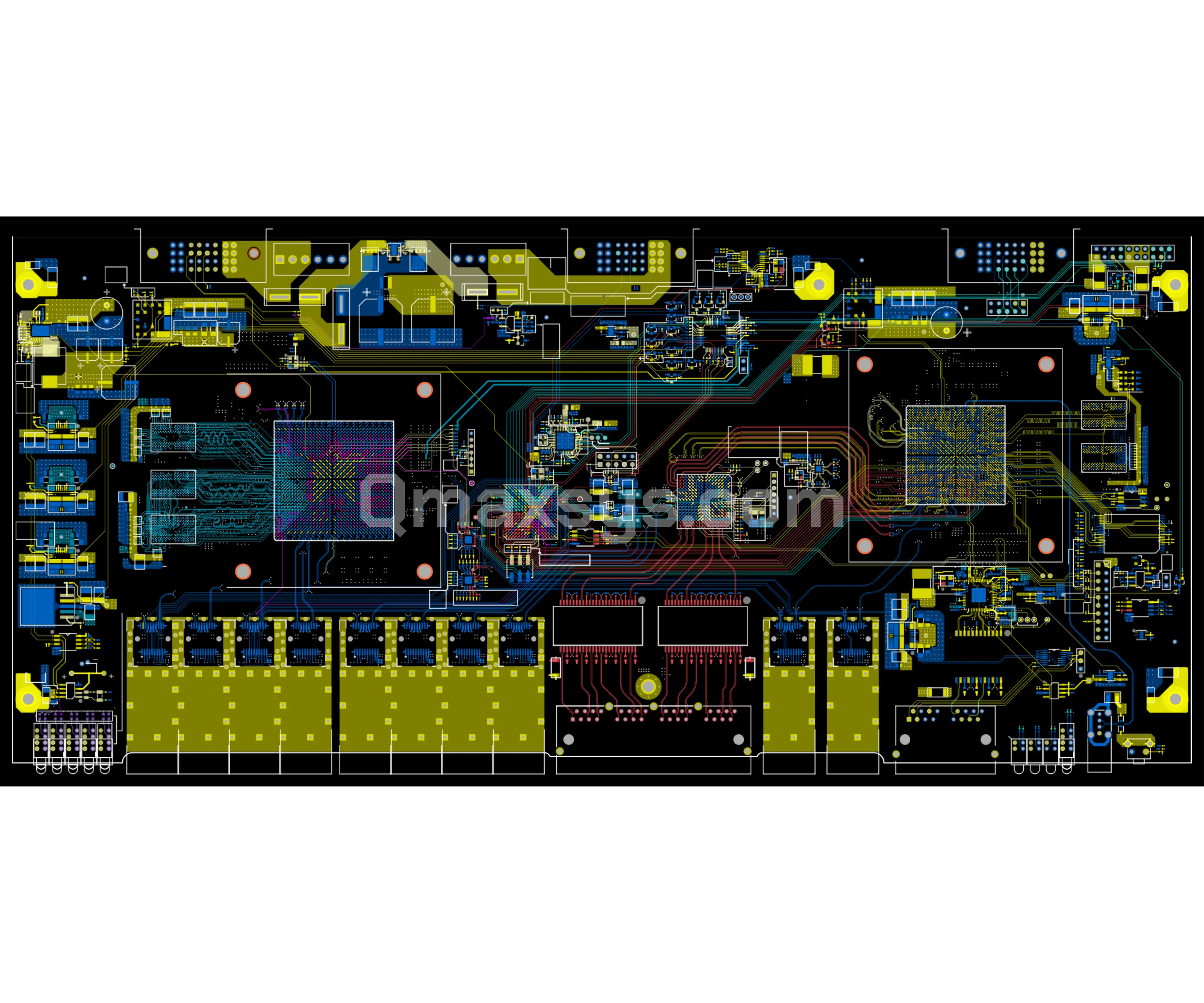
Qmax Systems partnered with a telecom networking equipment manufacturer to design a high-density, 20-layer printed circuit board for a multi-port fiber-optic access platform. Working from customer-supplied schematics, mechanical drawings, and a detailed bill of materials, Qmax's PCB design team translated a complex mixed-signal, high-speed digital architecture into a fully routed, manufacturing-ready Cadence Allegro board. The design integrates over 2,600 components, including multiple high pin-count BGA devices, DDR3 memory, and several power management ICs, on a compact double-sided layout. The fabricated board powered up and operated correctly at first bring-up with zero design defects, and was delivered on schedule to the customer's production timeline.
Application Brief
The end product is a compact, carrier-grade GPON Optical Line Terminal (OLT) used to deliver fiber-based broadband, voice, and video services to residential and business subscribers. The board combines a GPON access processor system-on-chip, an integrated Ethernet switch, and multiple physical-layer transceivers to aggregate traffic from fiber and copper uplinks onto multiple downstream optical ports. Because the platform is deployed in central-office and outdoor cabinet environments, the design demanded tight component placement, robust signal integrity across high-speed serial links, and a thermally efficient layout suitable for 24/7 continuous operation.
Qmax Scope
Qmax Systems delivered the complete PCB design scope for the GPON OLT platform, from initial schematic review through fabrication-ready release:
- Performed detailed schematic review to validate design intent before layout began
- Reviewed and updated the customer-supplied BoM for part availability, footprint accuracy, and DFM fit
- Worked closely with the customer through every design stage, from input capture to final release
- Defined stack-up requirements for a 20-layer board with 10 routing layers and 10 plane layers
- Performed component footprint creation and verification, followed by constraint-driven placement of 2,600 components across a 91.89 sq. in. routed area
- Routed high-speed memory, SerDes, and Ethernet PHY interfaces under length-matching and impedance rules
- Performed Signal Integrity (SI) and Power Integrity (PI) analysis to validate high-speed routing and power delivery
- Ran DFM checks aligned to the customer's preferred fabrication and assembly partners
- Executed full design rule checking and design verification, with the fabricated board powering up and operating correctly at first bring-up
- Generated complete fabrication and assembly documentation, including BoM, netlist, and drawing reports
Challenges & Resolutions
High component density
2,600 parts and 9,564 pins were placed within a constrained 14.5 x 6.4 inch keep-in by sequencing placement around the largest BGAs first
Mixed fine-pitch and large-pitch BGAs
Multiple 0.8 mm and 1.0 mm pitch BGA devices required dedicated escape and fan-out planning to avoid via congestion
20-layer stack-up complexity
A 10 routing / 10 plane layer stack-up was structured to balance signal integrity needs with overall board thickness of approximately 21 mils
High via count
7,963 vias were managed through systematic via stitching and selective backdrilling to control stub effects on high-speed layers
DDR3 memory routing
Length and skew matching across multiple DDR3 devices was achieved using topology-aware autorouting with manual tuning
Multi-rate SerDes interfaces
1G and 10G optical port differential pairs were routed with controlled impedance and minimized crosstalk on dedicated signal layers
Dense power distribution
Numerous point-of-load regulators required careful plane segmentation to avoid noise coupling into sensitive analog and clock circuits
Mixed-signal isolation
Clock generation, real-time clock, and sensor circuits were isolated from high-speed switching sections through layer assignment and guard routing
Connector and SFP cage placement
Optical module footprints and connectors were positioned to meet customer mechanical drawing clearances without compromising routing channels
First-pass design success
Thorough verification across 7,410 connections paid off when the fabricated board powered up and ran correctly at first bring-up, with zero design defects and a satisfied customer
Major HW Components
Broadcom GPON Access Processor SoC
BGA1369 package
Broadcom Multi-Port Ethernet Switch IC
BGA1440 package
Multiple Broadcom Quad/Multi-Port Gigabit Ethernet PHY Transceivers
Lattice MachXO2 CPLD/FPGA
Board-level logic and port control
DDR3 SDRAM Memory Devices
Multiple 2 Gb and 4 Gb parts
NAND Flash and SPI NOR Flash
Boot and firmware storage
Point-of-Load DC-DC and LDO Regulators
Distributed power delivery
Precision Clock Generator and Multiple Crystal Oscillators
I2C EEPROM, Real-Time Clock, I2C Bus Multiplexers, and Temperature Sensors
Battery-Backed Real-Time Clock and Supervisory/Reset ICs
Major Interfaces
Multiple 1G and 10G SFP/SFP+ optical port interfaces
Gigabit Ethernet combo copper/optical uplink ports
DDR3 memory interface to the access processor SoC
SGMII/serial high-speed links between switch and PHY devices
I2C management buses for optical module and sensor monitoring
SPI boot interface for flash memory
JTAG debug and programming interfaces
UART console interface for system debug
PCIe-capable boot configuration interface
Multiple regulated power rails distributed via dedicated plane layers
PCB Design Specifications
Summary
This engagement showcases Qmax Systems' ability to take customer-supplied schematics through to a fully verified, manufacturing-ready PCB design for a high-density, high-speed networking platform. By combining disciplined stack-up planning, SI/PI-driven signal integrity routing, and rigorous DFM and design verification, Qmax delivered a 20-layer, 2,000-plus component design that powered up and operated correctly at first bring-up, with zero design defects and a satisfied customer.
The project reflects Qmax's full-stack PCB design capability for telecom and networking customers requiring complex, mixed-signal, high-pin-count board designs — from schematic review and BoM validation through SI/PI analysis, DFM, and final release documentation.