Above a Few Hundred Megahertz, Copper Stops Being a Wire
Qmax Systems has laid out RF and microwave boards since 1997 — 29 years of transmission-line design, stack-up and substrate selection, launch and transition engineering, via fencing, shielding architecture, antenna feed and keep-out definition, and fabricator alignment on low-loss and hybrid builds. The designers are Electrical and Electronics Engineers holding IPC CID certification, which on RF work is the difference between designing a launch and placing a footprint.
Above a few hundred megahertz the board stops being interconnect and becomes a circuit element. A ground via a millimeter too far from a source pin adds inductance that shifts a match. A coax launch with the wrong geometry costs return loss the link budget assumed it had. A via transition between layers is a discontinuity unless it is fenced. An enclosure seam becomes a slot antenna at the third harmonic. These are geometry and materials problems, and they are settled in the stack-up and the layout — never in firmware and never in the chamber.
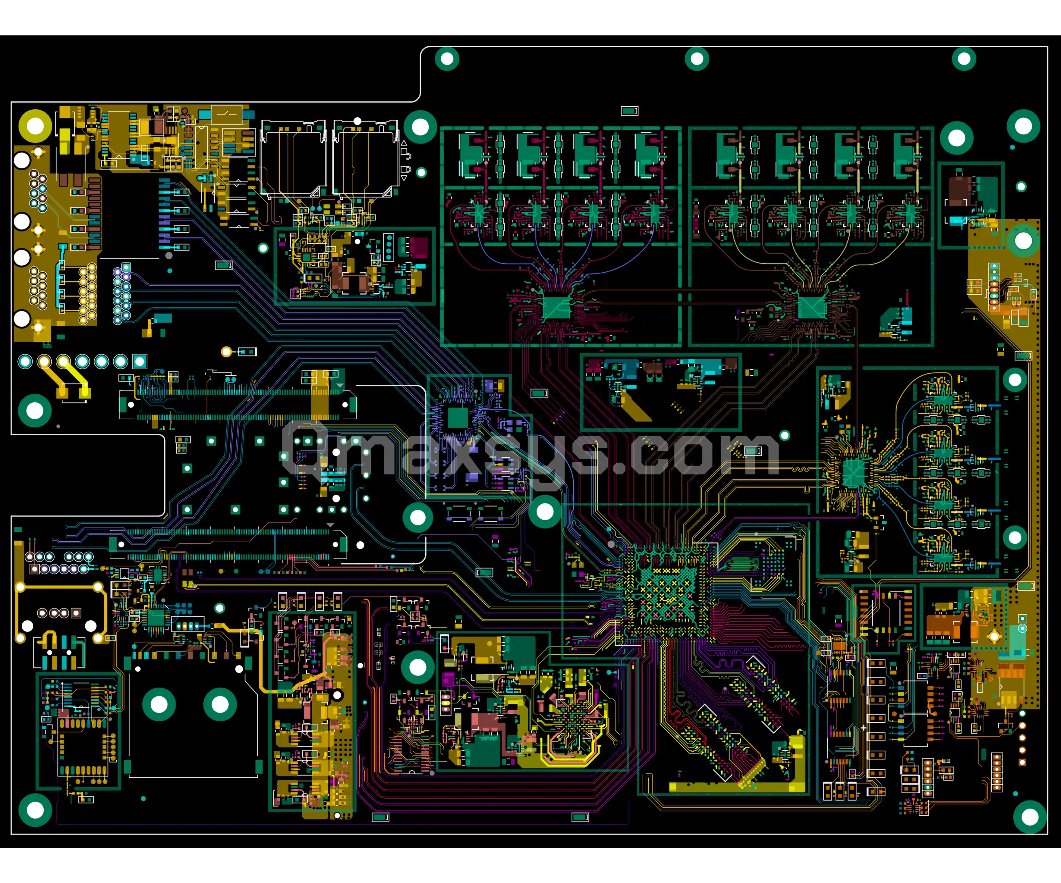
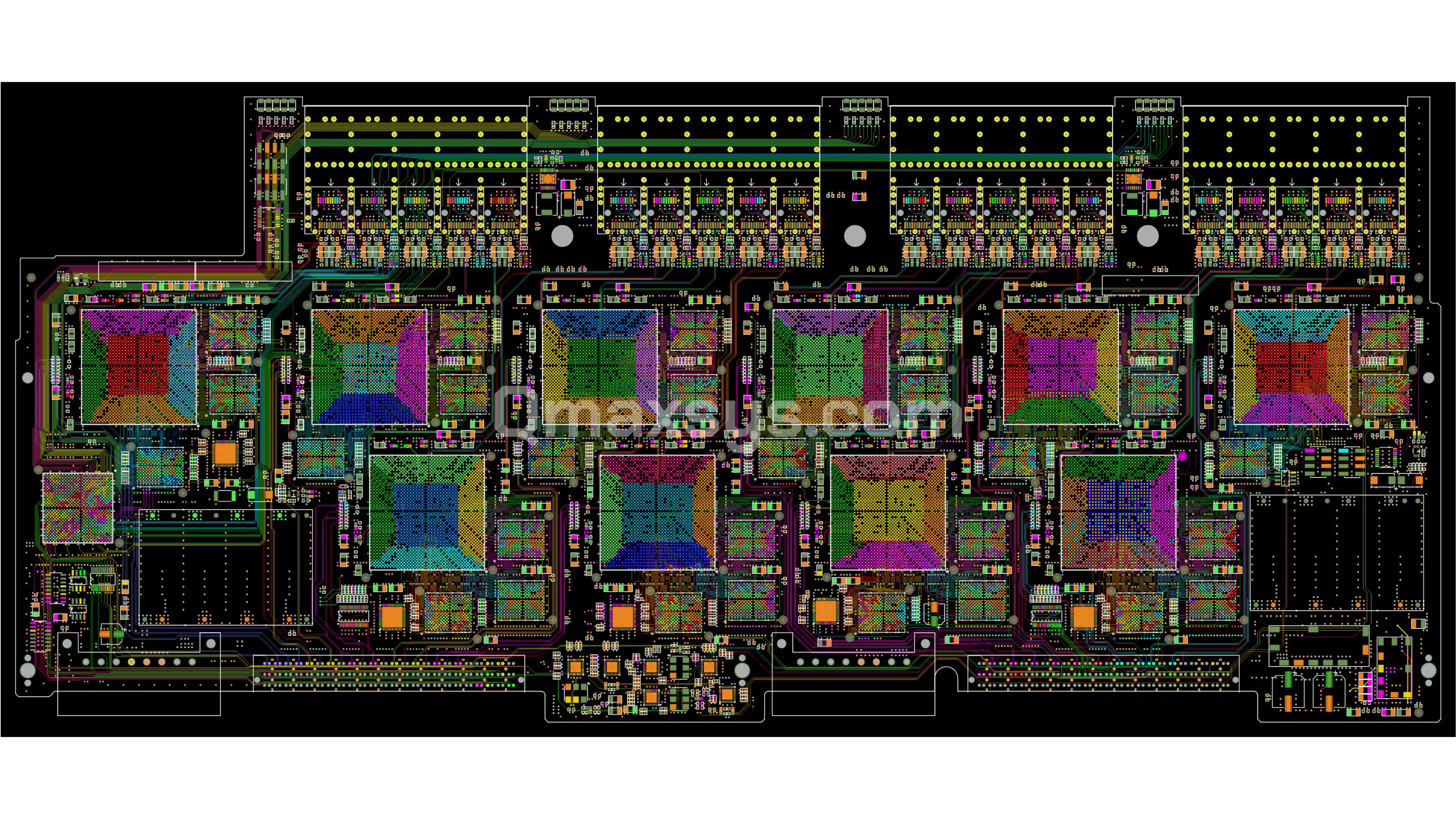
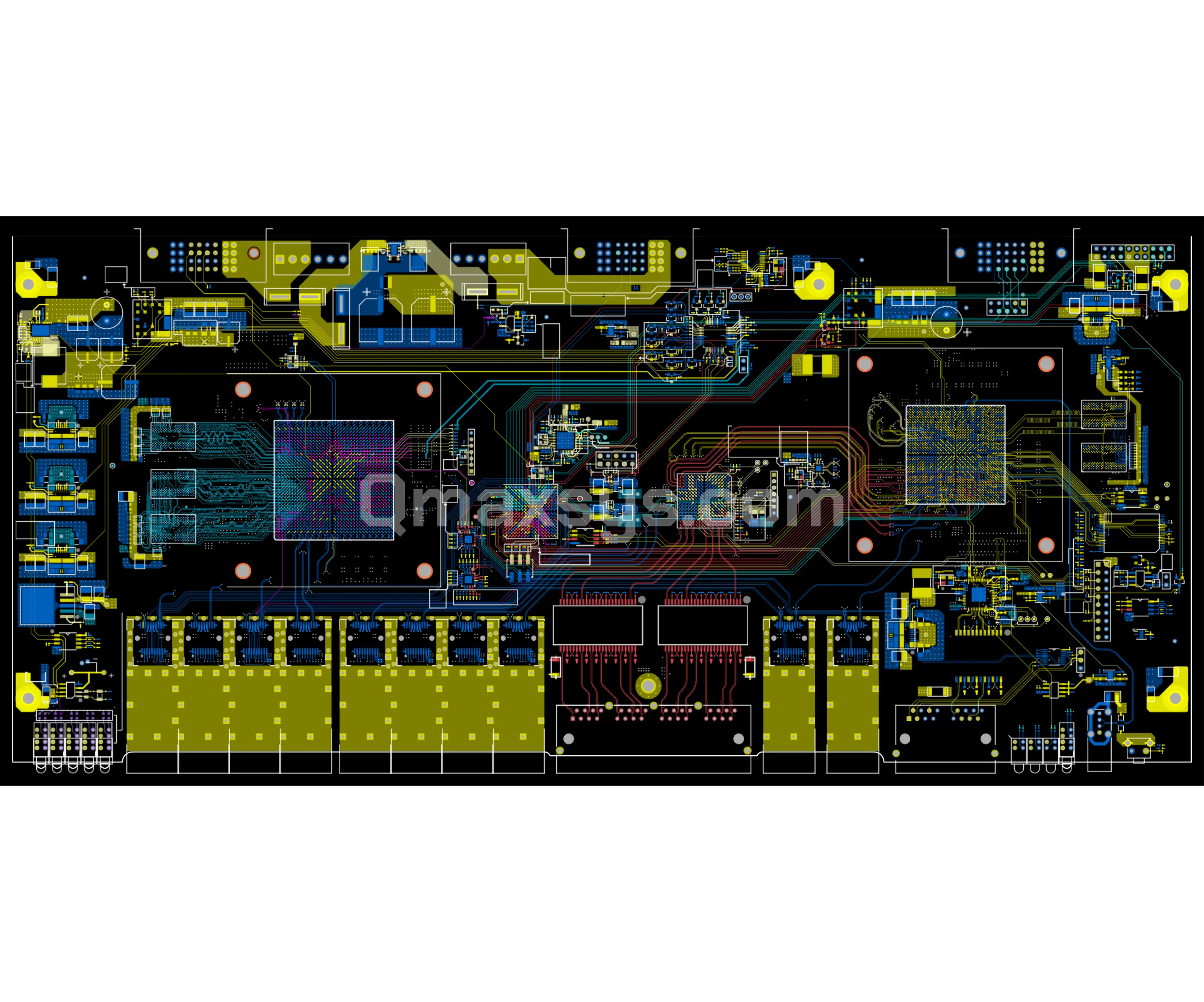
Delivered boards run from DC through mmWave and from milliwatt receive front-ends to kilowatt transmit stages: a 1 kW plasma generator at 13.56 MHz certified FCC Part 18 Class A, a 1 kW HF linear amplifier, a 12-antenna tri-band Wi-Fi 6 access point that passed FCC on first submission, and a wideband software-defined radio.
Feedlines, keep-outs, isolation targets, tuning against the real enclosure
Shielding Architecture
Shield cans, compartment walls, seam and aperture treatment with mechanical
Verification & Release
Coupons per lot, DFM and DFT review, Gerber or IPC-2581 package, IPC-6018
RF and Microwave Boards We Design
High-Power RF and Plasma Boards
Kilowatt-class transmit boards where the load is not 50 ohms and does not stay constant. The copper has to carry RF current without loss, spread device heat, and keep the sensing path clean enough to protect the output stage — all at once.
Directional coupler geometry for forward and reflected power sensing
Planar transformer construction on high-frequency laminate
Multi-layer shielding and compartment walls for kilowatt-class emissions
Device heat spreading and heat-sink interface at the board
Multi-Radio and Wireless Platforms
Boards where several radios must work simultaneously in one enclosure. The dominant layout problem is not any single radio but the interaction between them, and it is solved with separation, filtering and shielding rather than in software.
Wi-Fi 6, 6E and Wi-Fi 7 platforms with multi-band MIMO chains
Bluetooth, BLE, Thread and 802.15.4 coexistence layout
Cellular LTE and 5G NR module integration with GNSS
LPWAN and sub-GHz transceiver boards
Shielding partitions between radio sections on a shared board
Antenna Feeds and Integration
Feedlines, keep-outs and isolation designed against the enclosure, the ground plane and the mounting the product actually ships with. An antenna characterized on a bare board and then fitted into a metal housing is a different antenna.
Feedline design in microstrip, CPW and GCPW to the antenna port
Matching network placement and tuning on the assembled product
MIMO array layout with isolation and correlation targets
Keep-out definition and enclosure interaction analysis
Twelve-antenna platforms with three simultaneous bands
Receiver and Front-End Boards
Boards where the signal is near the thermal noise floor and every fraction of a decibel ahead of the first amplifier is lost permanently. Insertion loss before the LNA is the one loss no downstream gain recovers.
LNA-first receive chain layout with minimized pre-LNA loss
RF front-end modules with LNAs, mixers, filters and switches
Wideband transceiver layout with quadrature and clock separation
Low-noise supply and reference layout for RF sections
Shield-can provision over sensitive receive paths
Microwave and mmWave Boards
At millimeter-wave frequencies the mechanical design is part of the RF design. Launch geometry, keep-out compliance and radome material all change the measurement, and a keep-out violated by a couple of millimeters is visible in the result.
Carrier and sensing boards at 24 GHz, 60 GHz and 77 GHz
Controlled launch geometry and CPW antenna feeds for mmWave
Ultra-tight fabrication tolerance specification and coupon verification
Radome and enclosure material selection for transmission
Module integration with host interface, power and thermal
RF Instrumentation and Test Boards
Boards whose whole value is the accuracy of a measurement, where phase stability and repeatability matter as much as loss, and where the board itself must not contribute to what it is measuring.
Signal generator and sweep generator boards
RF power measurement and directional sensing boards
Phase-stable routing for measurement paths
Instrumentation boards with controlled impedance and low-loss laminate
Software-defined radio front-ends and amplifier chains
Board Complexity We Design To
Parameter
What we design to
Boards we have designed
Frequency coverage
DC through millimeter-wave, with substrate and geometry chosen per band rather than per board
13.56 MHz at 1 kW; tri-band 2.4 / 5.1 / 5.8 GHz; Wi-Fi 6E into 6 GHz; sensing boards at 24 GHz and 60 GHz
Power handling
Milliwatt receive front-ends through kilowatt transmit stages on the same discipline
1 kW at 13.56 MHz on LDMOS; a 1 kW HF linear amplifier; a 500 W low-frequency plasma stage
Base materials
Rogers 4350B and 4003C, Taconic TLY, Isola Astra, Megtron, PTFE and hybrid FR-4/PTFE per IPC-4103
Rogers islands set into FR-4 where only the RF section needed the material; a planar transformer built on Rogers laminate for a kilowatt stage
Transmission lines
Microstrip, stripline, coplanar waveguide and GCPW, modeled to impedance and insertion-loss budget
Twelve front-end chains routed to external antenna ports on one platform, each holding its own loss budget
Controlled impedance
50 Ω single-ended and 100 Ω differential per IPC-2141, with coupons on every lot
Coupon-verified on production platforms, because on thin low-loss laminate etch tolerance becomes the dominant impedance error
Transitions and via structures
Coax launches designed rather than inherited, layer transitions fenced, fence pitch set by the highest frequency present
Launch and transition geometry designed against the specific substrate in use rather than taken from a connector datasheet drawing
Layer count
2 to 36 layers available; RF boards are usually shallow with a carefully chosen reference structure
Low-layer radio boards through multi-layer platforms carrying twelve antenna chains and three simultaneous bands
Isolation and shielding
Shield cans and compartment walls designed from the block diagram, boundaries stitched at a frequency-appropriate pitch
Shielding over every RF section on a sealed outdoor access point, plus band-to-band filtering across three simultaneous radios
Antenna integration
Feedlines, matching geometry, keep-outs and isolation targets fixed against the real enclosure
Twelve antennas, three bands, 4×4 MIMO per band on a platform that passed FCC on first submission
Board qualification
Microwave boards inspected and tested to IPC-6018, bare board to IPC-6012 Class 2 or 3
IPC-6018 specified on RF builds, with IPC-6012 Class 2 or 3 on the remainder of the board
Millimeter-wave
Controlled launch geometry, CPW and GCPW feeds, tolerances tight enough that etch variation does not dominate
Delivered at 24 GHz and 60 GHz, with design practice extending to 77 GHz automotive radar bands
Applications & Real-World Project Experience
Antenna PCB integration for an outdoor tri-band Wi-Fi 6 access point, routing twelve front-end module chains and their RF interfaces to the external antenna ports with tuned matching and isolation for all-weather 802.11ax coverage.
Multi-radio RF layout for a connected EV VCU platform, with a dedicated radio board integrating BLE, LTE Cat 1, and GNSS modules plus antenna matching, isolated from high-current motor and switching loads on the companion ECU board.
EMI-conscious RF layout for a railway-grade lubrication controller, co-locating BLE and GSM modules with antenna placement and ground partitioning inside an IP65 track-side enclosure.
A transmission line is only as good as the reference plane under it. Impedance comes from the geometry and the substrate together, loss comes from the dielectric and the conductor surface, and both are decided at stack-up definition — where the laminate is selected on Dk and Df at the operating frequency rather than at 1 MHz.
Microstrip, stripline, CPW and GCPW modeled to impedance and loss budget
Substrate selected per IPC-4103 on Dk and Df at the operating frequency
Uninterrupted reference under every RF trace, enforced as a rule
Conductor loss modeled with skin effect and copper surface roughness included
Impedance held per IPC-2141 and verified with coupons on every lot
Every Transition Is a Designed Structure
Wherever an RF signal changes layer, changes medium or leaves the board, it meets a discontinuity. A coax launch, a layer-to-layer via, a connector footprint and a component pad are all structures with their own return loss, and each is designed rather than dropped in from a library and hoped for.
Coax-to-board launch geometry designed, not inherited from a footprint
Layer transitions fenced with ground vias placed against the frequency of interest
Return-path vias placed with the signal via at every transition
Component pad and antipad geometry tuned for the mounted part
Connector footprints optimized rather than taken from the datasheet drawing
Shielding and Coexistence by Geometry
In a multi-radio product the isolation budget is a layout budget. Separation, grounded copper, compartment walls and filter placement at the boundary are what deliver it, and none of them can be added after the enclosure is tooled. On twelve-antenna platforms this is the whole design.
Shield can and compartment wall provision designed in from the block diagram
Compartment boundaries stitched at a pitch chosen for the frequency, not by default
Antenna placement against measured isolation targets on the assembled product
Filtering placed where a conductor crosses a shield boundary
Enclosure seams and apertures treated jointly with mechanical design
Equipment class
United States
European Union
India
Intentional radiators — Wi-Fi, BLE, sub-GHz
FCC Part 15 Subpart C
RED 2014/53/EU with EN 300 328 and EN 301 893
WPC ETA, TEC MTCTE
Unintentional radiators — digital and IT equipment
FCC Part 15 Subpart B, Class A or Class B
EN 55032 emissions, EN 55035 immunity
CISPR 32 as adopted, via TEC and BIS
ISM RF equipment — plasma generators, RF heating
FCC Part 18
EN 55011 / CISPR 11, Group 2 Class A
CISPR 11 as adopted
Cellular and licensed radio
FCC Parts 22, 24 and 27, plus carrier and PTCRB acceptance
RED with EN 301 908
TEC MTCTE and WPC
RF exposure
SAR under 47 CFR 2.1093, or MPE evaluation
EN 50566, EN 62479 and EN 62311
Per DoT and TEC requirements
Automotive radar and e-mobility
FCC Part 15, with CISPR 25 at component level
UN ECE R10, with CISPR 25 at component level
AIS 004 (Part 3), certified through ARAI
The board itself
UL 796 with UL 94 V-0 laminate
IEC 61189 test methods
As adopted
Microwave board qualification
IPC-6018 inspection and test, IPC-6012 Class 2 or 3
Same, as contractually specified
Same, as contractually specified
How an RF Board Gets From Netlist to Release
The Errors Are Geometric and Invisible on a Schematic
An RF board fails because a ground via sat a millimeter too far from a source pin, because a launch was copied from a connector datasheet, because a via fence was pitched for 2.4 GHz on a 24 GHz line, or because a bracket landed in the near field.
Stage-gate checklists, each with a named owner and a recorded outcome
In-house scripts auditing fence pitch, reference continuity and keep-out compliance
Checks anchored to documents rather than to taste: IPC-2221 for generic design, IPC-4103 for high-frequency materials, IPC-6012 and IPC-6018 for board and microwave qualification, IPC-A-600 and IPC-A-610 with J-STD-001 for acceptability, IPC-2231 for design-for-excellence
Release Is Read Aloud by Two People
One engineer reads the item, a second confirms the state out loud — a flight-crew checklist, deliberately. On an RF board the item most often waved through is the material call-out, and a board fabricated on the wrong laminate is scrap rather than a rework.
Challenge and response on every release item, spoken and confirmed
Material, thickness and impedance targets cross-read against the loss budget
Coupon requirement and keep-out geometry confirmed present on the drawing
Sign-off recorded against a name, not just a date
What Lands in Your Hands
A release package that carries the material and tolerance requirements an RF board lives or dies by, not just its copper. You own all of it.
Gerber and drill data, or IPC-2581 (DPMX) and ODB++
Fabrication drawing with substrate call-out, thickness, impedance table and coupon requirement
Assembly drawing with shield-can, compartment and antenna keep-out geometry
BoM, netlist and IPC-D-356 bare-board test data
IPC-6018 inspection and test requirement stated where applicable
Native CAD source files in the tool the design was built in
Stage
What it means on this kind of board
What has to be true before it closes
1Requirement Capture
Band plan, power level per stage, how many radios must work simultaneously, and the enclosure — needed early, not late
The mechanical model is in hand, because on an RF board the housing is part of the circuit
2Library Development
RF component footprints tuned for the mounted part, connector launch lands designed rather than copied
Land patterns conform to IPC-7351 and BGA practice to IPC-7095, and every RF footprint has been reviewed against its own datasheet geometry
3Design Environment Setup
Substrate and thickness fixed first, then the stack-up built around them; impedance targets and coupon spec set
The material is available in the chosen partner's process, and the impedance target is achievable in their etch control
4Component Placement
RF chains separated, shield-wall positions fixed, antenna keep-outs frozen for the mechanical team
Isolation between chains is designed rather than hoped for, and mechanical has the keep-outs it must respect
5PCB Routing
Transmission lines with uninterrupted reference, via fencing along them, transitions and launches designed individually
No RF trace crosses a reference discontinuity, and every transition is a structure somebody designed
6Impedance and Response Analysis
Impedance and loss against budget, matching network response, harmonic and filter behavior
Every line meets its insertion-loss and VSWR target on paper before a board exists
7Design Verification
DRC and ERC, keep-out compliance in 3D, fence pitch against the highest frequency, seam and aperture review with mechanical
The enclosure has been reviewed as an RF component, not just as a box
8Manufacturing Outputs
Substrate call-out, impedance table, coupon requirement, IPC-6018 test requirement, fabrication and assembly drawings
The partner cannot build it on the wrong material or skip the coupon
Why Choose Qmax for RF and Microwave PCB Design
Kilowatts and Microvolts From One Team
RF layout is one strand of our full PCB design capability, the same designers lay out 1 kW LDMOS transmit stages and receive front-ends working near the thermal noise floor. That range is the point: the shielding and grounding discipline needed to keep a kilowatt out of a sensitive receiver is exactly the discipline that makes a twelve-antenna multi-radio product behave in a sealed enclosure.
Compliance Engineered, Not Discovered
The shield boundary and the filter list are drawn with the block diagram, and every conductor crossing that boundary is filtered by design. Pre-compliance screening then runs in house while the board can still change — which is how an outdoor access point with twelve antennas in a sealed housing passed FCC on first submission.
Impedance Verified, Not Assumed
Controlled-impedance test coupons are specified on every lot, because on thin low-loss laminate etch tolerance becomes the dominant impedance error and an untested assumption is an untested product. Trace width, laminate and the partner's etch capability are chosen together rather than in sequence.
Engineers Who Design the Launch Rather Than Place It
A connector land pattern from a datasheet is a starting point, and knowing that is the difference between an RF designer and a drafter. The Qmax team are Electrical and Electronics Engineers holding IPC CID certification, awarded by IPC rather than asserted. The founder still lays out boards, 38 years after starting on hand-taped artwork.
Matched to a Partner That Stocks the Material
Qmax works with verified fabrication partners across the United States, Japan, South Korea, Taiwan and India. On RF work the partner has to handle PTFE and low-loss lamination, hold impedance on thin substrate, supply coupons per lot, and actually have the laminate — which is a much shorter list than the one a standard multilayer uses.
ISO 9001 and ISO 13485, and 100% Your IP
Design work runs inside certified quality systems with the document control and traceability that medical and regulated programs require. A mutual NDA precedes any technical discussion, files are held under role-based access rather than on shared drives, and you own every schematic, layout, library and simulation file at every milestone. Qmax retains no rights and reuses nothing across clients.
Get a Complimentary Consultation with Our RF and Microwave PCB Experts
A one-hour session with a senior Qmax PCB design engineer. Bring a band plan, a mechanical model, or a board that is failing emissions or missing its match. You will get a view on where the loss went and what the substrate needs to be — not a proposal.
PCB design work spans DC through millimeter-wave. Delivered boards include a 1 kW stage at 13.56 MHz, tri-band platforms at 2.4, 5.1 and 5.8 GHz, Wi-Fi 6E into the 6 GHz band, and sensing boards at 24 GHz and 60 GHz, with design practice extending to the 77 GHz automotive radar bands. On power, the range runs from receive front-ends near the thermal noise floor to kilowatt transmit stages.
What substrates does Qmax Systems specify for RF boards?
Rogers 4350B and 4003C, Taconic TLY, Isola Astra, Megtron, PTFE and hybrid FR-4/PTFE builds, specified per IPC-4103 for high-frequency applications. Selection is made on Dk and Df at the operating frequency rather than at 1 MHz, because a laminate that looks acceptable on a datasheet headline can be the dominant loss term at 6 GHz. Hybrid construction is used where only part of the board needs the expensive material — a Rogers island for the RF section on an otherwise FR-4 board is often the right economic answer, and it is a stack-up decision agreed with the fabricator.
How tightly can Qmax Systems hold controlled impedance?
50 Ω single-ended and 100 Ω differential as standard, designed per IPC-2141 and correlated with the fabricator's actual process before layout rather than taken from a generic calculator. Controlled-impedance test coupons are specified on every lot, because on an RF board an untested impedance assumption is an untested product. On thin low-loss laminate a 50 Ω line can be narrow enough that etch tolerance becomes the dominant impedance error, which is why the trace width, the laminate and the shop's etch capability are chosen together rather than in sequence.
Why does a via transition need a via fence?
Because a signal changing layers leaves its reference plane and has to find a new one, and the current that returns along the old plane needs a path to the new one. Without nearby ground vias that return current takes a long detour, which adds inductance, creates a discontinuity in the transition and radiates. A via fence gives the return current a short path and simultaneously provides shielding along the line. The fence pitch is chosen against the highest frequency of interest — a spacing that works at 2.4 GHz is transparent at 24 GHz — rather than set by a default rule.
How does Qmax Systems design a coax-to-board launch?
As a structure, not as a footprint. A connector's recommended land pattern is a starting point, not an optimized launch: the ground via ring position, the pad geometry, the antipad diameter on the reference plane and the taper into the transmission line all affect return loss, and the manufacturer's drawing is drawn for a generic stack-up rather than yours. The launch is designed against the specific substrate and thickness in use, with the ground return path from the connector shell into the board plane made short and symmetric. On a high-power board the launch also has to carry RF current without loss, which makes copper and plating a factor as well as geometry.
How does Qmax Systems prevent desense in multi-radio boards?
By treating it as a layout budget rather than a test-stage discovery. Every radio combination is analyzed for the frequency relationships that cause trouble — harmonics, intermodulation products, and receive bands sitting on a neighboring transmitter's spectral skirt. The remedies are all physical: filter chains between bands, measured antenna isolation targets, deliberate spatial separation, compartment walls between radio sections, and keeping the processing subsystem and its switching supplies out of receive paths. A twelve-antenna tri-band access point and a twelve-antenna Wi-Fi 6E appliance were both laid out this way.
What does Qmax Systems do differently on kilowatt-class RF boards?
The copper stops being a signal path and becomes a power path as well. It has to carry RF current with low loss, spread the device heat into the heat-sink interface, and keep the sensing path clean enough to protect the output stage — because on a plasma generator the reflected-power measurement is what triggers VSWR foldback, and if it is slow or noisy the device dies. Directional coupler geometry is designed for defined directivity, detection is placed close to the coupler, and the sensing routing is shielded and physically separated from the power stage. A planar transformer built on Rogers laminate handles the magnetics.
Does Qmax Systems design antenna feeds and integration?
Yes. Feedlines are designed in microstrip, CPW or GCPW to the antenna port; matching network geometry and component placement are laid out for tuning; keep-outs are defined and the mechanical design is then held to them; and MIMO arrays are laid out against isolation and correlation targets. Tuning is done on the assembled product rather than on a bare board, because an antenna characterized in free space and then fitted into a metal housing is a different antenna, usually by several decibels. On the outdoor access point that meant twelve chains, three bands and a sealed enclosure — and a first-submission FCC pass.
How does Qmax Systems account for copper roughness and skin effect?
Both are in the loss model at the operating frequency rather than assumed away. Skin effect confines current to a shrinking surface layer as frequency rises, so conductor loss increases and the effective cross-section is far smaller than the geometric one. Surface roughness then lengthens the actual path current takes along that surface, adding loss a smooth-conductor model underestimates — which is why low-profile copper is specified where the budget is tight. Both feed substrate selection and trace geometry at stack-up definition, and the stack-up is correlated with the fabricator before layout begins.
What changes at millimeter-wave frequencies?
The mechanical design becomes part of the RF design. Radome thickness and material change the transmitted signal; a mounting bracket in the near field changes the pattern; a keep-out violated by two millimeters is visible in the measurement; and fabrication tolerance that was irrelevant at 2.4 GHz becomes the dominant impedance error. The board work is controlled launch geometry, CPW and GCPW feeds, keep-out definition the mechanical design is held to, and tolerances specified tightly enough that etch variation does not dominate — verified with coupons on every lot. Boards are inspected and tested to IPC-6018.
Can Qmax Systems fix a board that failed FCC or CE?
Yes, and it is one of the most frequent RF engagements. The approach is to identify the coupling path by measurement before changing anything, because remediation aimed at the wrong mechanism costs a revision and buys nothing. Pre-compliance screening locates the offending frequency, then near-field investigation and selective disconnection establish whether energy is leaving on a cable, through an enclosure seam, or from the board itself. The deliverable is a diagnosis with evidence and costed options — frequently a filter change, a bonding or seam fix, or a re-layout of one section rather than a new board. Where a redesign genuinely is required, Qmax says so and explains why.
What in-house RF capability supports the layout work?
A vector network analyzer for S-parameters, matching and VSWR on assembled hardware; spectrum analyzers for harmonics, spurious emissions and radiated and conducted pre-screening; a Rohde & Schwarz CMW500 for radio conformance and modulation quality; oscilloscopes for control-loop and bias behavior; and thermal cameras for RF device and heat-spreader temperature mapping. Formal certification runs at accredited laboratories.
Can Qmax Systems take our RF schematic and own the layout?
Yes, and most RF engagements start that way. A signal-chain review runs first, because on an RF board the schematic often understates the problem — a matching network drawn without reference to the physical length it will occupy, a filter placed where its ground return cannot be short, or a sensing tap taken from a node that will not be quiet once laid out. Work is delivered in Altium Designer, Cadence Allegro and OrCAD, Siemens Xpedition and PADS, Zuken or KiCad, and native source files are handed back in the tool the design was built in.
Which fabricators can build RF stack-ups?
Fewer than can build a standard multilayer, which is why the shop is chosen before layout rather than after. Low-loss and PTFE materials need specific lamination processes and handling; hybrid FR-4/PTFE builds need a shop comfortable with mixed-dielectric construction; and tight impedance tolerance on thin substrate needs demonstrated etch control. Qmax agrees material availability, stack-up and impedance tolerance with the fabricator up front, specifies controlled-impedance coupons for per-lot verification, and will work with your preferred shop provided the build is genuinely inside their process.
What information does Qmax Systems need to quote an RF layout?
Schematics or a netlist, the mechanical outline with antenna and connector positions, the BoM, and then the four things that size the job: the band plan and the frequencies involved, the power levels at each stage, how many radios have to work simultaneously, and the markets the product ships into. The enclosure matters more than on any other board type, so mechanical drawings or a 3D model are needed early rather than late. An NDA is signed before any technical discussion.