The Stack-Up Decides the Board Before the First Trace Is Drawn
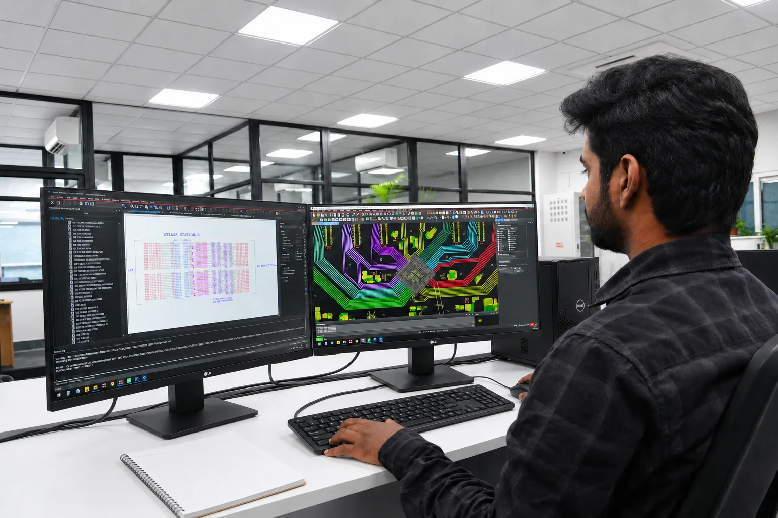
Qmax Systems has laid out high-speed digital boards since 1997 — 29 years of stack-up definition, escape routing, length and skew matching, via engineering, controlled-impedance work, signal and power integrity analysis, DFM release and fabricator alignment. The designers are Electrical and Electronics Engineers holding IPC CID certification, which matters on a board like this because deciding where the escape goes is an engineering judgment rather than a drafting task.
Above a few gigabits per second a board stops being interconnect and becomes part of the channel. A via turns into a stub, a plane split turns into a discontinuity, a glass bundle in the laminate turns into skew, and a 2,597-ball BGA turns into a routing problem that either fits inside the layer budget or does not. None of that is visible on the schematic. All of it is decided in the stack-up, the escape plan and the via strategy, and all of it is cheaper to decide before layout than to discover afterwards.
Delivered work runs to 36 layers, 4,623 components, more than 36,000 pins, roughly 25,000 through-vias on a single card, 400 GbE of line-side capacity and 3.2 Tbps switch fabrics. Six of those boards reached Gerber release or first bring-up with no electrical re-spin, and more than 95% of Qmax high-speed designs reach production without a second spin for electrical issues.
Design Input Review
Schematic review, netlist and BoM audit, constraint capture before layout starts
Stack-Up Definition
Layer assignment, laminate selection per IPC-4101, impedance targets correlated with the fab
Constraint Development
Net classes and routing rules derived from pre-layout analysis, not from rules of thumb
Placement & Floor Planning
BGA-first placement, escape planning, thermal and mechanical coexistence
High-Speed Routing
Length and skew matching, reference continuity, differential pair and bus topologies
Via & HDI Engineering
Microvia structures per IPC-2226, via protection per IPC-4761, backdrill definition
SI & PI Analysis
Pre-layout budgeting and post-layout confirmation of channels and power delivery
DFM & Release
DFM, DFA and DFT review, fabricator alignment, Gerber or IPC-2581 package
High-Speed Boards We Design
Backplanes, Fabrics and Line Cards
Chassis-based platforms where dozens of high-speed pairs have to cross a connector and hold their eye across the backplane. These are the densest boards Qmax builds and the ones where the layer budget is fixed by the card-slot pitch before layout begins.
Backplanes and midplanes to 14 line-card slots
ATCA blades and carrier-class line cards to 36 layers
Fabric SerDes escape and AC-coupled backplane transitions
Redundant −48 V telecom feed and hot-swap sequencing layout
Server, Compute and AI Accelerator Boards
Motherboards and carriers around server-class silicon, where a very large BGA, a high-current PDN and a fabric of PCIe lanes all compete for the same layers, and the thermal solution constrains placement before routing starts.
Multi-processor motherboards for x86 and Arm server silicon
PCIe switch fabrics with bifurcation, hot-plug and per-slot control
2,397-ball and larger BGA escape on fine-pitch geometry
Memory Subsystems
Fly-by DDR topologies and SRAM arrays where timing closure is a routing problem. Byte-lane matching, address and command fan-out and reference continuity all have to hold across dozens of devices, not just one.
Fly-by DDR3, DDR4, LPDDR4X and DDR5 topologies
Multi-device arrays to 48 DDR3 devices on one board
QDR-II SRAM packet-buffer and lookup arrays
Byte-lane, address and command length and skew matching
HDI, ELIC and Advanced Construction
Where the escape cannot be achieved in through-hole construction, the answer is microvia. Qmax designs the full progression from a single microvia tier to any-layer interconnect, and specifies it so the fabricator can actually build it.
HDI Type I, II and III per IPC-2226
Stacked and staggered microvias, any-layer ELIC
Via-in-pad with conductive fill per IPC-4761
Rigid-flex construction per IPC-2223 and IPC-6013
Networking, Optical and Telecom Interfaces
Front-panel port density and the optical cage placement that goes with it, plus the timing distribution that carrier equipment depends on and enterprise equipment usually does not.
SFP+, SFP28, QSFP and QSFP-DD cage placement and escape
10G, 25G, 40G and 100G port banks with matched attachment
GPON and optical access platform layout
Low-jitter LVPECL clock trees and IEEE 1588 timing distribution
Embedded, FPGA and Edge Compute Boards
Smaller boards where the same high-speed discipline applies at lower layer count, and where cost and size are as much a constraint as margin. A four-layer board with a DDR interface is still a high-speed board.
FPGA carrier boards with bank-aware I/O and transceiver clocking
System-on-module carriers and single-board computers
Cost-constrained 4 to 8 layer designs with DDR and Gigabit Ethernet
USB4, Thunderbolt 4 and HDMI routing with ESD and EMI containment
Board Complexity We Design To
Parameter
What we design to
Boards we have designed
Layer count
2 to 36 layers, rigid, flex, rigid-flex and HDI
36 layers on an ATCA blade — the deepest stack-up in the portfolio. Also 30, 28, 24 and 20-layer boards in production
Routing and plane budget
Split assigned to the channel count and the power delivery network, never to a default ratio
16 routing over 20 plane at 36 layers; 14 over 16 at 30; 12 over 16 at 28; 10 over 10 on a 20-layer optical platform
Trace and space
Down to 3.5 mil on released production designs, finer inside HDI construction
3.5 mil traces carrying 144 lanes of PCIe Gen5 on a 20-layer motherboard that released with no re-spin
Drill and via structures
Through, blind, buried, stacked and staggered microvia, any-layer ELIC, via-in-pad with conductive fill, backdrill for stub removal
Roughly 25,000 through-vias on one 24-layer card; 10,300+ at 30 layers; 7,963 with selective backdrill at 20 layers
Device escape
Fine-pitch BGA fan-out planned before placement, mixed pitches given separate escape plans
2,597-ball BGAs escaped on 3.5 mil geometry; mixed 0.8 mm and 1.0 mm pitch resolved on a 60-pins-per-square-inch board
Board thickness
Thin flex builds through backplane-class construction, aspect ratio confirmed with the partner
121 mil at 36 layers and 127 mil at 30 layers — thick enough that plating aspect ratio is itself a constraint
Controlled impedance
Single-ended and differential targets per IPC-2141, verified with coupons on every lot
Held across 96 length-matched SerDes pairs at 30 layers, and across 40 optical port channels at 24 layers
Interface rates
DDR3 through DDR5 and LPDDR5X; PCIe Gen3 through Gen5; 10G, 25G and 56G SerDes; USB4 and Thunderbolt 4
144 lanes of PCIe Gen5 at 32 GT/s for 3.2 Tbps aggregate; 96 SerDes pairs; 40 × 10GbE for 400 GbE line-side
Memory density
Fly-by topologies with byte-lane, address and command matching across many devices
A 48-device DDR3 array on one board, and a 32-device fly-by array split across two network processors
Base materials
High-Tg FR-4 and low-loss laminates per IPC-4101, HDI and microvia materials per IPC-4104, selected on loss at the operating frequency
Low-loss laminates on backplane-class boards; FR-4 at 2.5 mm on a 20-layer carrier-grade optical platform
Applications & Real-World Project Experience
Controlled-impedance routing on a 30-layer terabit-scale switch fabric card, holding tight single-ended and differential targets across 96 length-matched SerDes pairs carrying ~3.2 Tbps of aggregate bandwidth.
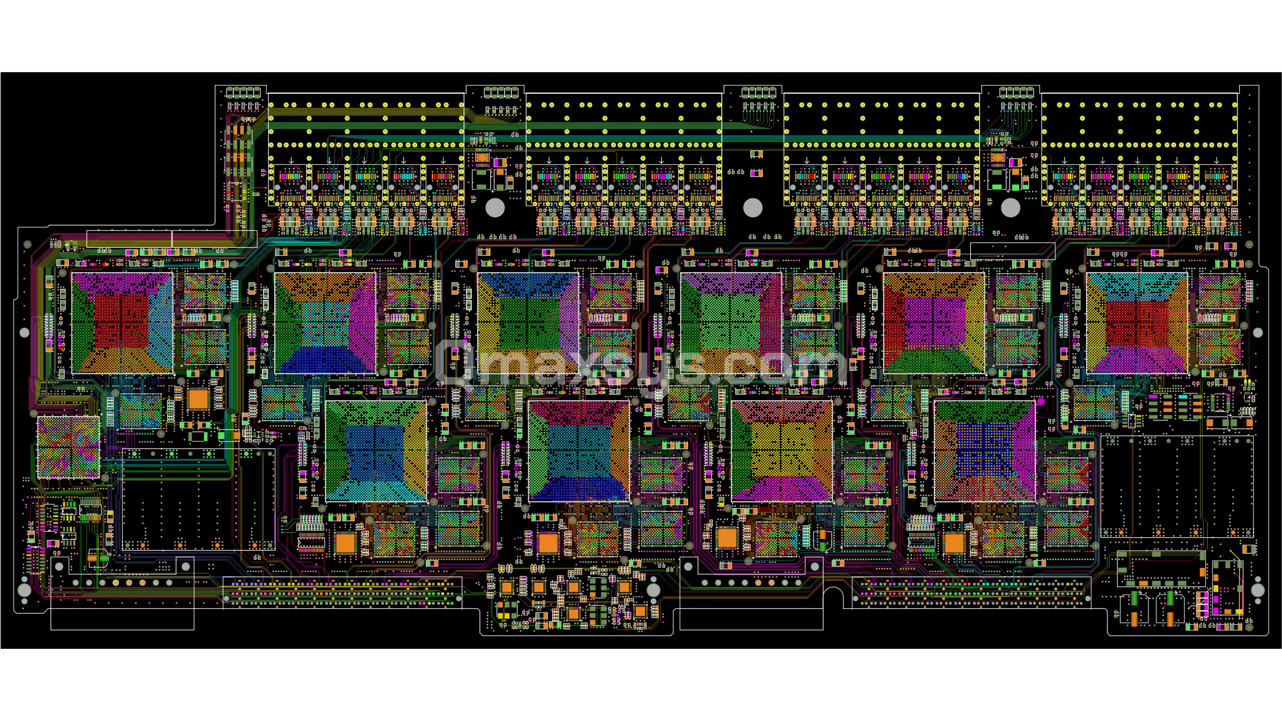
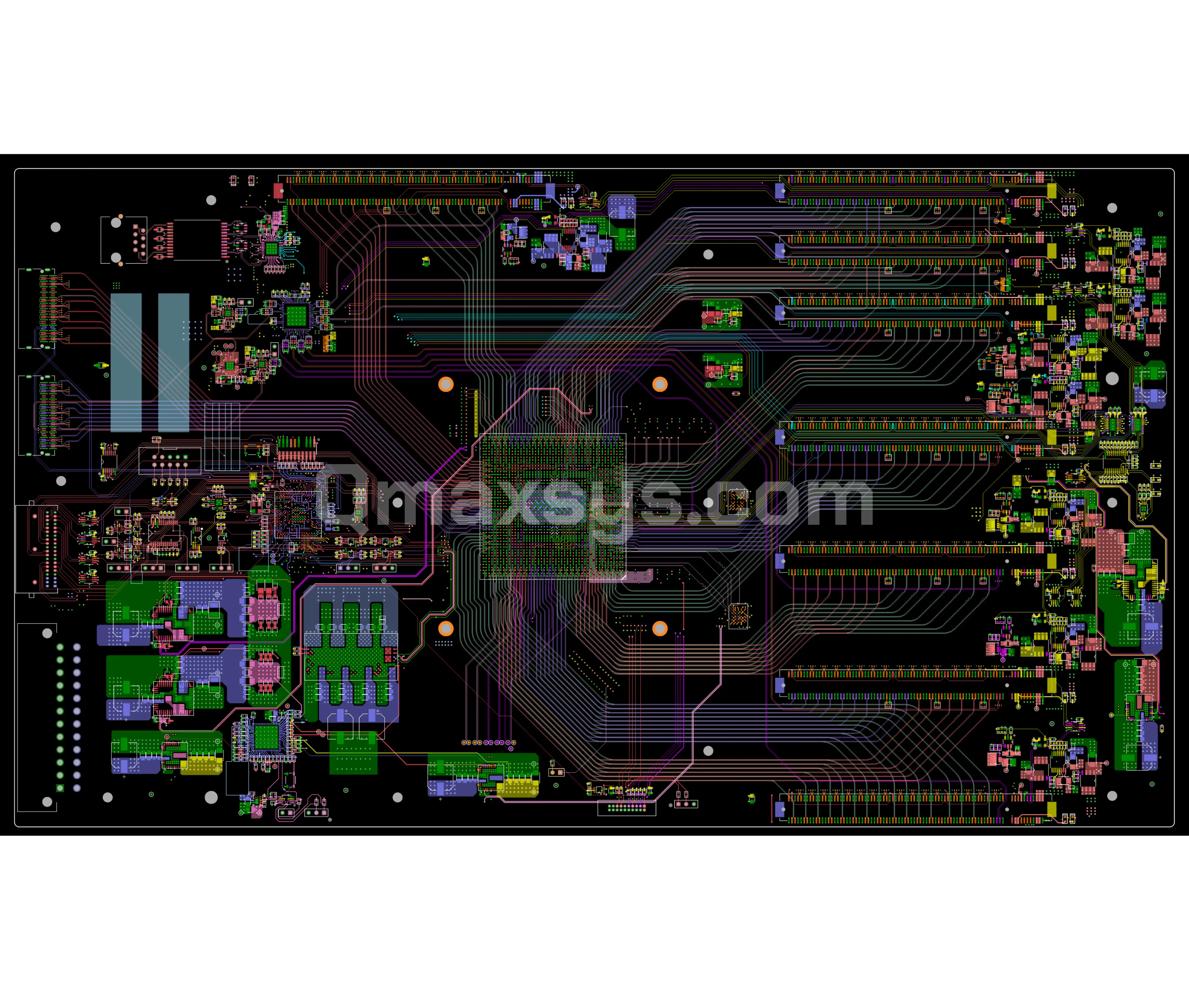
Twenty-layer high-density layout for a PCIe Gen 5 AI GPU expansion chassis motherboard, with high pin-count BGA escape routing, HDI microvia structures, and a 144-lane fabric-switch interconnect - released to Gerber with zero DFM re-spins.
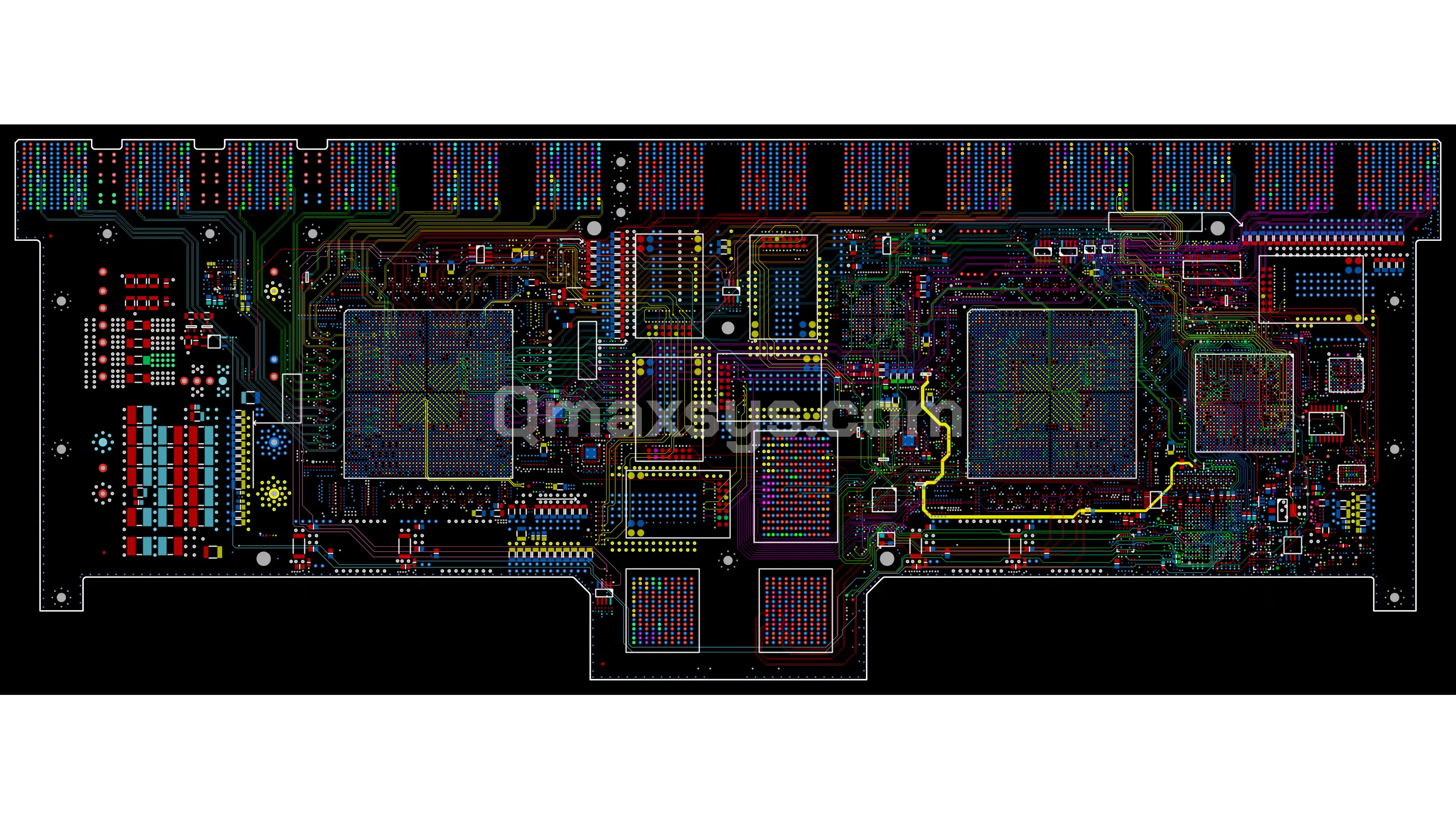
Pre- and post-layout signal integrity analysis for a 36-layer dual-NPU ATCA packet-processing line card, covering dense fabric SerDes channels and a 32-device DDR3 array, validated to Gerber release without a re-spin.
High-speed memory routing on a 24-layer 40-port 10GbE core-router line card, with length-matched, controlled-impedance topologies across a 30-device QDR-II SRAM packet-buffer array supporting 400 GbE aggregate line-side capacity.
Twenty-layer high-frequency PCB design for a carrier-grade GPON Optical Line Terminal, routing the Broadcom GPON access-processor SoC and multi-port switch fabric to first-pass bring-up with zero design defects.
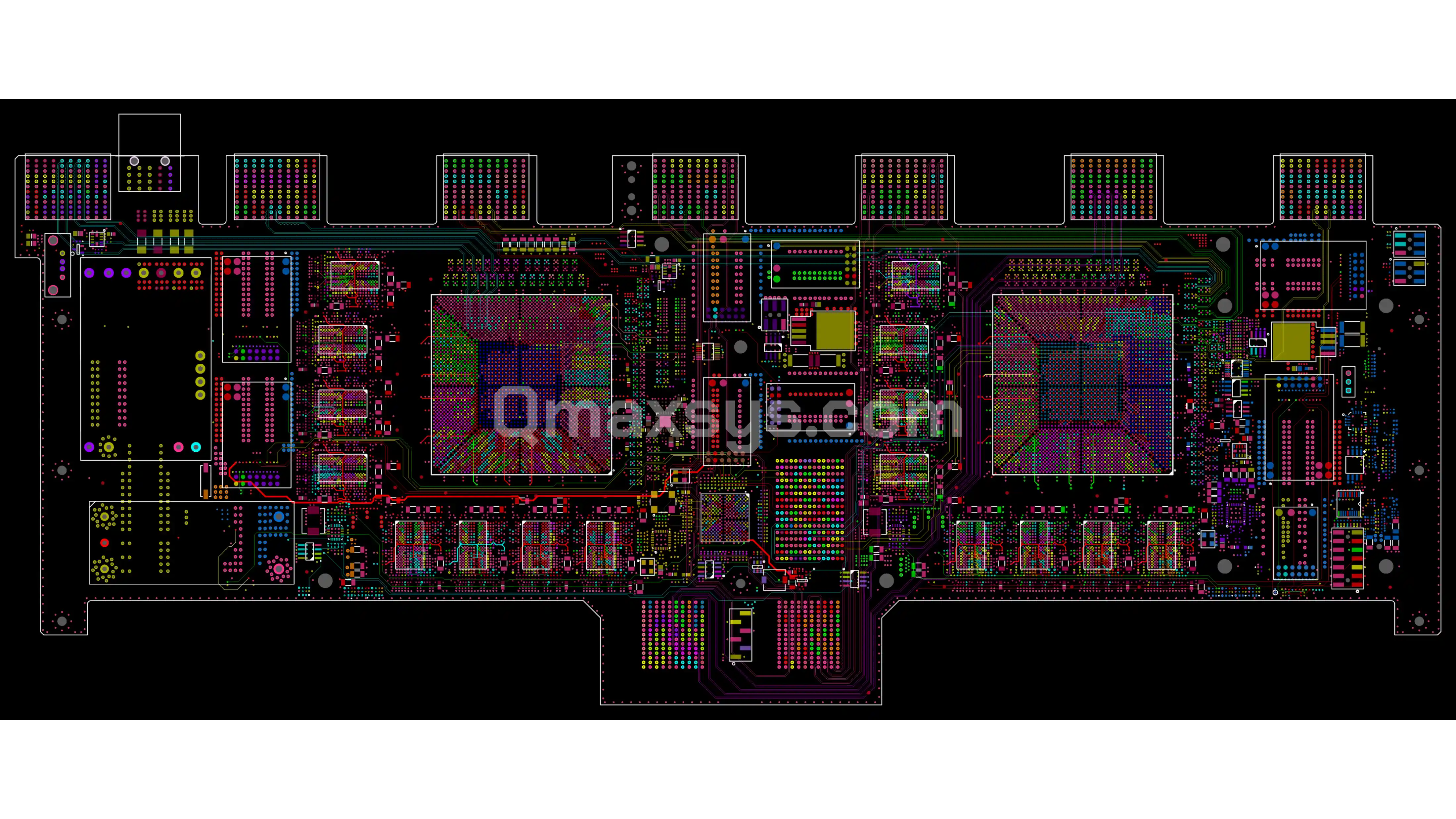
Differential-pair routing and length matching on a 28-layer multi-FAP packet-processing line card - the platform's most component-dense board - spanning four Broadcom PETRA-B fabric access processors and a 48-device DDR3 array, delivered without a re-spin.
The stack-up fixes the layer budget, the impedance achievable, the loss per inch and the via aspect ratio, and it is agreed with the fabricator before layout opens. Above roughly 10 GHz the laminate stops being a cost line and becomes an electrical parameter, so it is selected on Dk and Df at the operating frequency rather than at 1 MHz.
Layer assignment driven by the channel count and the PDN, not by a default ratio
Laminate selected per IPC-4101 on loss at the operating frequency
Impedance targets per IPC-2141, correlated with the fabricator's process
Glass-weave skew mitigated by spread-glass style or routing angle
Aspect ratio checked against the fabricator's plating capability before release
Escape Routing as the Real Constraint
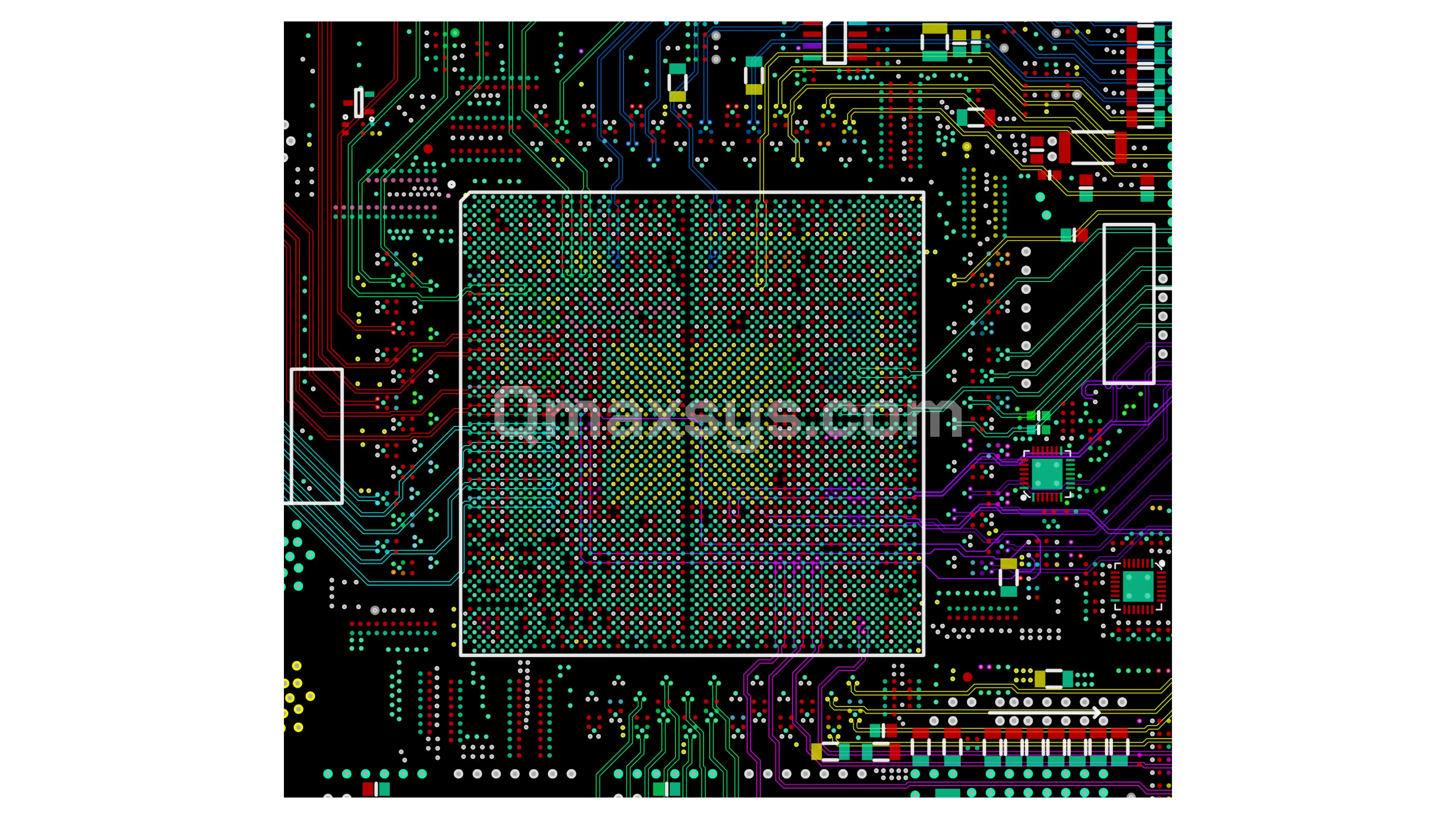
On a 2,597-ball BGA the difficult part is not the trace, it is getting out of the ball field at all. Escape planning determines the layer count and therefore the cost of the board, which is why placement starts with the largest devices and works outward rather than starting at the connectors.
Largest BGAs placed and escaped first, then everything else fits around them
Bank-aware and pin-swap-aware fan-out to shorten and simplify the escape
Via-field and antipad strategy that keeps routing channels open
Land patterns to IPC-7351 and BGA design practice to IPC-7095
Mixed 0.8 mm and 1.0 mm pitch handled with separate fan-out plans per device
Vias Engineered, Not Placed
At multi-gigabit rates a via is a discontinuity with a stub attached. Which via type appears where is a deliberate decision balancing electrical performance, fabrication yield and cost — and on a 127 mil board it is also a mechanical decision, because aspect ratio limits what can be plated reliably.
Backdrill applied to remove stubs on signals above roughly 10 Gbps
Stacked and staggered microvias, and any-layer ELIC, per IPC-2226
Via-in-pad with conductive fill per IPC-4761 where escape demands it
Return-path vias placed with the signal via, not left to the plane to sort out
Via stitching used deliberately for reference continuity and for shielding
Analysis
When it runs
What it decides
Pre-layout channel budgeting
Before floor planning
Layer count, laminate, maximum routed length, connector choice
Stack-up and impedance definition
With the fabricator, before layout
Trace geometry, impedance tolerance, aspect ratio feasibility
Escape and floor plan review
Before routing opens
Whether the design fits the layer budget at all
Post-layout SI extraction
On the routed database
Sign-off against the budget, while a re-route is still free
PDN impedance and DC IR drop
On the routed database
Decoupling BoM, plane shapes, via counts, regulator placement
Yield risk, aspect ratio, backdrill depth, assembly and test access, against IPC-6012 class and IPC-A-600
Why Choose Qmax for High-Speed PCB Design
More Than 95% First-Time-Right
High-speed work is one of four layout disciplines inside our PCB design services practice. Over 95% of Qmax high-speed designs reach production without a second spin for electrical issues, and six of the boards on this page closed with no re-spin at all — at 36 layers, at 28,445 pins, at 3.2 Tbps. Routing constraints are derived from analysis before layout rather than discovered by iteration afterwards.
Escape Routing Is Where the Cost Lives
On a 2,597-ball BGA the binding constraint is not the trace, it is getting out of the ball field — and that decides the layer count, which decides the price of every board you ever build. Qmax places the largest devices first and proves the escape fits before routing opens, which is why boards land on the layer count that was quoted.
CID-Certified Engineers, Not Draftsmen
Every Qmax PCB designer is an Electrical or Electronics Engineer who can read the circuit, and the team holds IPC CID certification — externally awarded, not self-declared. Several designers have close to forty years at the board, and the founder still designs, with 38 years that began on hand-taped artwork and now covers 36-layer HDI.
A Library That Has Already Made the Mistakes
30,000+ component library parts, every symbol, footprint and 3D model validated against the manufacturer datasheet through a 7-stage independent QC process, land patterns to IPC-7351 and BGA footprints to IPC-7095. On a high-pin-count board the library is where a scrapped build comes from, and NVIDIA has used Qmax 3D models for GPU thermal simulation.
Routed to the Partner That Can Hold It
Qmax works with verified fabrication partners across the United States, Japan, South Korea, Taiwan and India. A high-layer-count board is routed to a shop with demonstrated aspect-ratio and backdrill control rather than to whoever quoted lowest, and the specification is agreed with them before layout rather than after.
ISO 9001 and ISO 13485, and 100% Your IP
Design work runs inside certified quality systems with the document control and traceability that medical and regulated programs require. A mutual NDA precedes any technical discussion, files are held under role-based access rather than on shared drives, and you own every schematic, layout, library and simulation file at every milestone. Qmax retains no rights and reuses nothing across clients.
Get a Complimentary Consultation with Our High-Speed PCB Experts
A one-hour session with a senior Qmax PCB design engineer. Bring a netlist, a stack-up proposal, or a channel that will not close its eye. You will get an opinion on what the layer count really needs to be — not a proposal.
What is the highest layer count Qmax Systems has designed?
36 layers — 16 routing layers over 20 power and ground planes at 121 mil finished thickness, on an ATCA packet-processing blade carrying 4,623 components and 19,705 pins. Also in production: a 30-layer switch fabric at 127 mil, a 28-layer line card of 172 square inches, a 24-layer card with more than 36,000 pins, and several 20-layer platforms. Routine work spans 2 layers to 36 across rigid, flex, rigid-flex and HDI construction, designed to IPC-2221 and its sectional standards and specified to IPC-6012 or IPC-6013 Class 2 or Class 3.
What data rates and interfaces does Qmax Systems route?
Delivered work includes PCIe Gen5 at 32 GT/s across 144 lanes for 3.2 Tbps aggregate, 96 differential SerDes pairs on a 30-layer fabric, 40 × 10GbE optical ports for 400 GbE of line-side capacity, and fly-by DDR3 and DDR4 arrays up to 48 devices on a single board. DDR5, LPDDR5X, PCIe Gen6 and higher-rate PAM4 signaling are part of current design practice — the stack-up, loss modeling and via engineering all extend to them — and where a program needs those rates the same budgeting discipline applies.
Why does Qmax set routing constraints before layout instead of checking afterwards?
Because analysis that runs after layout can only confirm or condemn, while analysis that runs before it changes the design while changing it is still free. Pre-layout channel budgeting allocates insertion loss across package, board, connector and cable, and states what is left for the routing — which then fixes layer count, trace geometry and maximum length before the first net is placed. Post-layout extraction then verifies the routed database against that same budget. A discrepancy at that point is a re-route, which costs a day; the same discrepancy found at bring-up costs a fabrication cycle.
How does Qmax Systems handle escape routing on very large BGAs?
Placement starts with the largest devices and works outward, because on a 2,597-ball BGA the binding constraint is getting out of the ball field, and that constraint sets the layer count and therefore the cost of the board. The plan covers bank-aware and pin-swap-aware fan-out, via-field and antipad strategy that keeps routing channels open, and separate escape plans per device where pitches are mixed — the GPON platform combined 0.8 mm and 1.0 mm pitch BGAs and each needed its own approach to avoid via congestion across 7,963 vias. Land patterns follow IPC-7351 and BGA practice follows IPC-7095.
What HDI and microvia construction does Qmax Systems design?
The full progression, per IPC-2226: HDI Type I, II and III, stacked and staggered microvias, and any-layer interconnect (ELIC) where every layer connects to every other through copper-filled microvias. Via-in-pad with conductive fill is designed per IPC-4761, and it was used on the 20-layer PCIe Gen5 motherboard to make the Gen5 escape fit at 3.5 mil trace geometry. HDI is specified only where through-hole construction genuinely cannot achieve the escape, because it costs yield and money — and it is specified in terms the fabricator can build rather than as a general aspiration.
When does Qmax Systems use backdrilling?
On signals above roughly 10 Gbps, and on thick boards where the unused portion of a through-via becomes an electrically significant stub. A stub is a resonant structure: at high enough frequency it presents a notch in the channel that no equalization recovers. Backdrill removes it by controlled-depth drilling after plating. On the 20-layer GPON platform selective backdrilling controlled stub effects on the high-speed layers while leaving the rest of the board in cheaper standard construction. Depth, tolerance and remaining-stub length are all specified in the fabrication drawing rather than left to the shop.
How does Qmax Systems manage fiber-weave skew?
Laminate is a woven composite, so the dielectric constant a trace sees varies with whether it runs over glass bundle or over resin. On a long differential pair that variation becomes skew, and skew becomes closed eye. Two mitigations are used, chosen on cost: specify a spread-glass or mechanically-spread fabric style so the weave is more uniform, or route the pair at an angle to the weave so both conductors average the same dielectric. On very long channels both are applied. The choice is made at stack-up definition, with the fabricator, because it is a material and fabric-style decision rather than a routing decision.
Does Qmax Systems perform signal integrity and power integrity analysis in-house?
Yes, and both run before layout release rather than after it. Signal integrity covers channel budgeting, S-parameter extraction, eye and jitter analysis and crosstalk allocation as a routing rule. Power integrity covers PDN target impedance derived from the actual current step, DC IR drop across plane shapes, via-count sizing for current, and decoupling placement checked for anti-resonance gaps. On the AI GPU motherboard that meant designing a 100 A PDN alongside a 144-lane Gen5 fabric in the same 20 layers.
What controlled-impedance tolerance can Qmax Systems hold?
Single-ended 50 Ω and differential 85, 90 or 100 Ω targets are standard, designed per IPC-2141 and correlated with the fabricator's actual process before layout rather than taken from a generic calculator. Controlled-impedance test coupons are specified on the fabrication drawing so every lot is verified rather than assumed, and the impedance table and drill table are part of the release package. On the 30-layer fabric those targets were held across 96 length-matched SerDes pairs; on the 24-layer card, across 40 optical port channels.
Can Qmax Systems work from our schematics in our CAD tool?
Yes, and it is the most common engagement on this page. On all six boards above the customer supplied verified schematics, a mechanical outline, a BoM and constraint information, and Qmax owned the stack-up, floor plan, routing, analysis and fabrication release. Work is delivered in Altium Designer, Cadence Allegro and OrCAD, Siemens Xpedition and PADS, Zuken or KiCad, and native source files are handed back in the tool the design was built in so it stays maintainable by your team. A schematic review is run first, because the fastest way to lose a week is to route a schematic error faithfully.
How does Qmax Systems coordinate with the fabricator?
Before layout, not at quotation. The stack-up and impedance targets are agreed with the chosen fabrication house so the design is buildable in their process rather than in a generic one, and aspect ratio, backdrill capability, minimum drill and plating limits are all confirmed against that shop. Qmax works with several of the world's leading fabricators, will work with your preferred shop, and specifies controlled-impedance coupons for per-lot verification. DFM findings are resolved with the shop directly rather than passed back and forth through the customer.
What does the release package contain?
Gerber and drill data, or IPC-2581 (DPMX) and ODB++ where preferred; a fabrication drawing carrying the stack-up, impedance table and controlled-impedance drill table; an assembly drawing; BoM; netlist and IPC-D-356 bare-board electrical test data; impedance and worst-case tolerance analysis; DFM, DFA and DFT review records; the design verification checklist; and the native CAD source files. The intent is a package complete enough that the fabricator and assembler need to ask nothing.
How does Qmax Systems keep emissions under control at the layout stage?
By deciding where return current flows before routing, and by treating every conductor that leaves the board as a potential antenna. Reference continuity is enforced at each plane transition, return vias are placed with their signal vias, clock and edge-rate energy is kept off interfaces that exit the enclosure, and filtering is placed where a conductor crosses the shield boundary. Designs are worked against CISPR 32 / EN 55032 and EN 55035, with FCC Part 15 Subpart B Class A or Class B as the US basis. In a compact product the dominant coupling path is usually a cable rather than the PCB, so cable entry and segregation are treated as layout decisions.
Can Qmax Systems take over a board that failed bring-up or compliance?
Yes, and it is a regular engagement. The first step is diagnosis rather than redesign: review the stack-up, constraint set and routed database against the measured symptom, then prove the mechanism before changing anything. Failures at these rates trace to a small set of causes — a discontinuous return path, an un-backdrilled stub, a decoupling gap at the frequency the load actually excites, weave skew on a long pair, or a channel that was never budgeted. The deliverable is a diagnosis with evidence and costed options, which is often a re-route of one region rather than a new board.
What information does Qmax Systems need to quote a high-speed layout?
Schematics or a netlist, the mechanical outline with connector and mounting positions, the BoM, the interfaces and data rates involved, the target layer count if one is already assumed, the fabricator if one is chosen, the performance class the product needs, and the markets it ships into. If the constraint set does not exist yet, Qmax writes it as a first deliverable — that is normal rather than exceptional. An NDA is signed before any technical discussion.