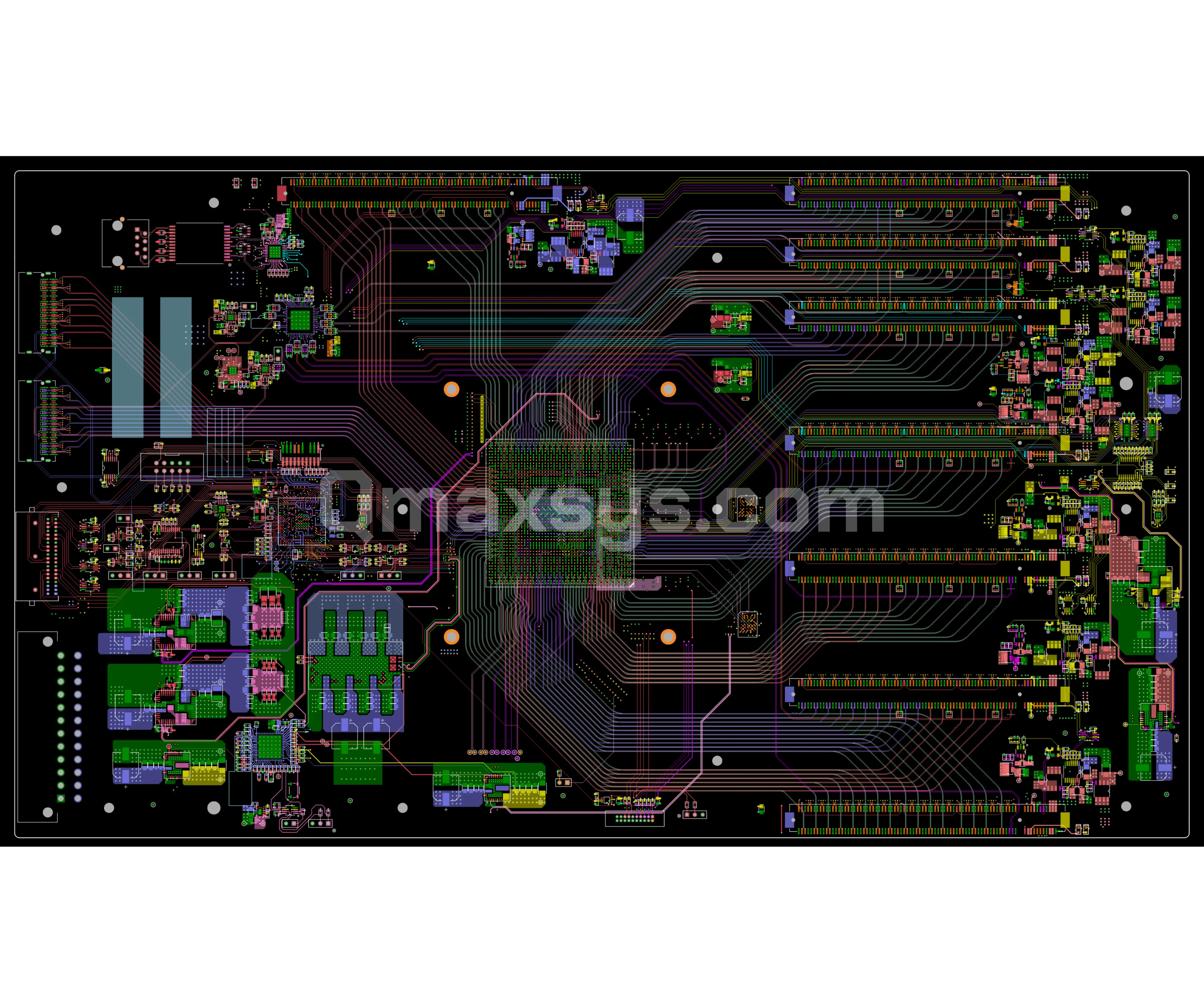
High-Density AI GPU Expansion Chassis Motherboard
Project Overview
Qmax Systems was engaged to provide end-to-end PCB design services for a high-density AI GPU expansion chassis motherboard targeting next-generation AI datacenter and HPC deployments. The board serves as the central PCIe Gen 5 switching and chassis management plane, aggregating multiple GPU expansion slots through a 144-lane PCIe Gen 5 fabric switch and providing per-slot hot-plug management, multi-rail power delivery, and a full I²C/SMBus management topology.
Application Brief
The board is deployed inside a composable AI infrastructure chassis used to pool and dynamically allocate GPU resources across multiple host servers in an AI datacenter environment. The platform targets AI inference, HPC compute, composable NVMe storage, and financial analytics workloads that demand deterministic, high-bandwidth PCIe connectivity.
The chassis motherboard must sustain up to 3.2 Tbps of aggregate PCIe Gen 5 bandwidth while supporting hot-swap insertion and removal of expansion cards under live system conditions — placing stringent requirements on signal integrity, power sequencing, and thermal management at the PCB level.
Qmax Scope
Qmax Systems provided end-to-end PCB design services covering the full design lifecycle from requirements capture through fabrication data release:
- Customer requirements capture and schematic entry in collaboration with the customer's hardware engineering team
- Full PCB layout in Cadence PCB Editor (20-layer, controlled-impedance stackup)
- Signal integrity (SI) review for PCIe Gen 5 and other high-speed interfaces
- PCB design review against IPC standards and customer design rules
- DFM review conducted jointly with the contract EMS partner
- Executed full design rule checking and design verification, with the fabricated board powering up and operating correctly at first bring-up
- Generated complete fabrication and assembly documentation, including BoM, netlist, and drawing reports
Engineering Challenges
2,397-Pin BGA Breakout on a Dense 20-Layer Board
The PEX89144's 47.5 × 47.5 mm, 2,397-pin BGA (1.0 mm pitch) required a multi-layer escape strategy. Via-in-pad with conductive fill was used for the inner ball rows, enabling all 144 PCIe Gen 5 lanes to escape through layers 2–4 without impacting the top-layer routing channels for peripheral ICs.
PCIe Gen 5 Signal Integrity at 32 GT/s
At 32 GT/s, the PCIe Gen 5 channel budget allows very limited loss margin. Minimum trace widths of 3.5 mil and inter-layer via transitions were optimised through back-drilling simulation to keep insertion loss within the 36 dB limit specified in the PCIe Gen 5 CEM specification.
8-Slot Hot-Plug Power Management
Coordinating inrush control, power sequencing, and fault isolation across 8 independent hot-plug channels required careful placement of the LTC4210 controllers and their associated current-sense resistors to minimise loop inductance and ensure consistent 12 V ramp profiles within PCIe hot-plug timing requirements.
100 A PDN in a Server-Class Form Factor
Delivering 100 A to the PCIe switch core at low voltage demanded a tightly coupled PDN with four dedicated power planes, via arrays at each power domain boundary, and a carefully optimised capacitor placement hierarchy from bulk polymer tantalum down to 0201 MLCCs at the BGA.
Key Silicon & Component Highlights
PEX89144-DS106 (BGA-2397)
144-lane PCIe Gen 5 fabric switch — core routing silicon; 47.5 × 47.5 mm BGA with 2,397 pins on 1.0 mm pitch
MPM3695GBH-100-0001 (BGA-253)
100 A multiphase integrated power module — primary VR for the PCIe switch
LTC4210-1IS6 × 8
Hot-plug controller per expansion slot — manages 12 V inrush and slot power sequencing
PCA9548APW
8-channel I²C multiplexer — management bus root for all expansion slots
Major Interfaces
PCIe Gen 4 ×144 Lanes (16 GT/s)
Eight downstream x16 GPU expansion slot connectors and two upstream host x16 connectors routed through the PEX89144 fabric switch; differential pairs at 85 Ω, length-matched per lane and per bundle.
I²C / SMBus Management Bus
Hierarchical 3-tier topology: PCA9548 root mux → per-slot PCA9510 buffers → slot cards; covers GPU slots 1–8, NIC slots 1–2, host slots 1–2, PCIe switch (PEX_IIC4), IO card (I2C3), and BMC management channel (IIC0).
100 MHz PCIe Reference Clock (Differential)
9ZXL1231 12-output buffer distributing reference clocks to all slot connectors; GPIO-controlled mux (CLK0/CLK1 select) allows switching between on-board 9FGV1002 oscillator and external clock source.
1GbE Ethernet — RJ45 via HX5008NL Magnetics
Out-of-band management Ethernet port driven by BCM54213PE, with galvanic isolation, 25 MHz crystal reference (X2, X3), and independent analog power domain.
12 V Hot-Swap Power Inputs (J25, J26)
Dual power feed connectors feeding the LTC1647-3 hot-swap controllers and cascaded LTC4210-1 per-slot controllers; each slot provides independent 12 V, 3.3 V, and AUX 3.3 V rails with test points TP78–TP85.
Design Specifications
Summary
Qmax delivered a complete, fabrication-ready PCB design package within the agreed programme schedule. The Gerber release passed all fabrication DFM checks at the EMS partner without requiring a re-spin. The SI review confirmed that all PCIe Gen 5 channels met the insertion loss and impedance targets prior to prototype build.
This project demonstrates Qmax's capability to manage the full complexity of a 20-layer, high-density, high-speed PCB design from schematic to Gerber — encompassing state-of-the-art PCIe Gen 5 routing, multi-thousand-pin BGA breakout, and rigorous SI-driven design closure.