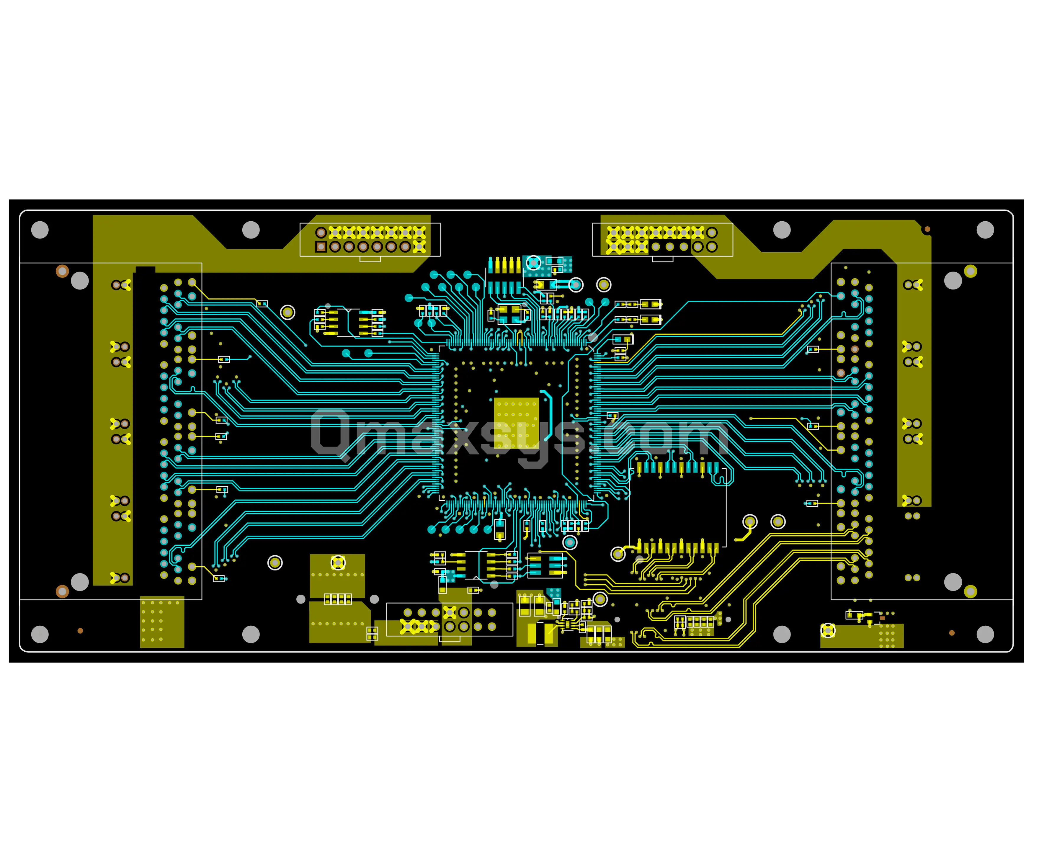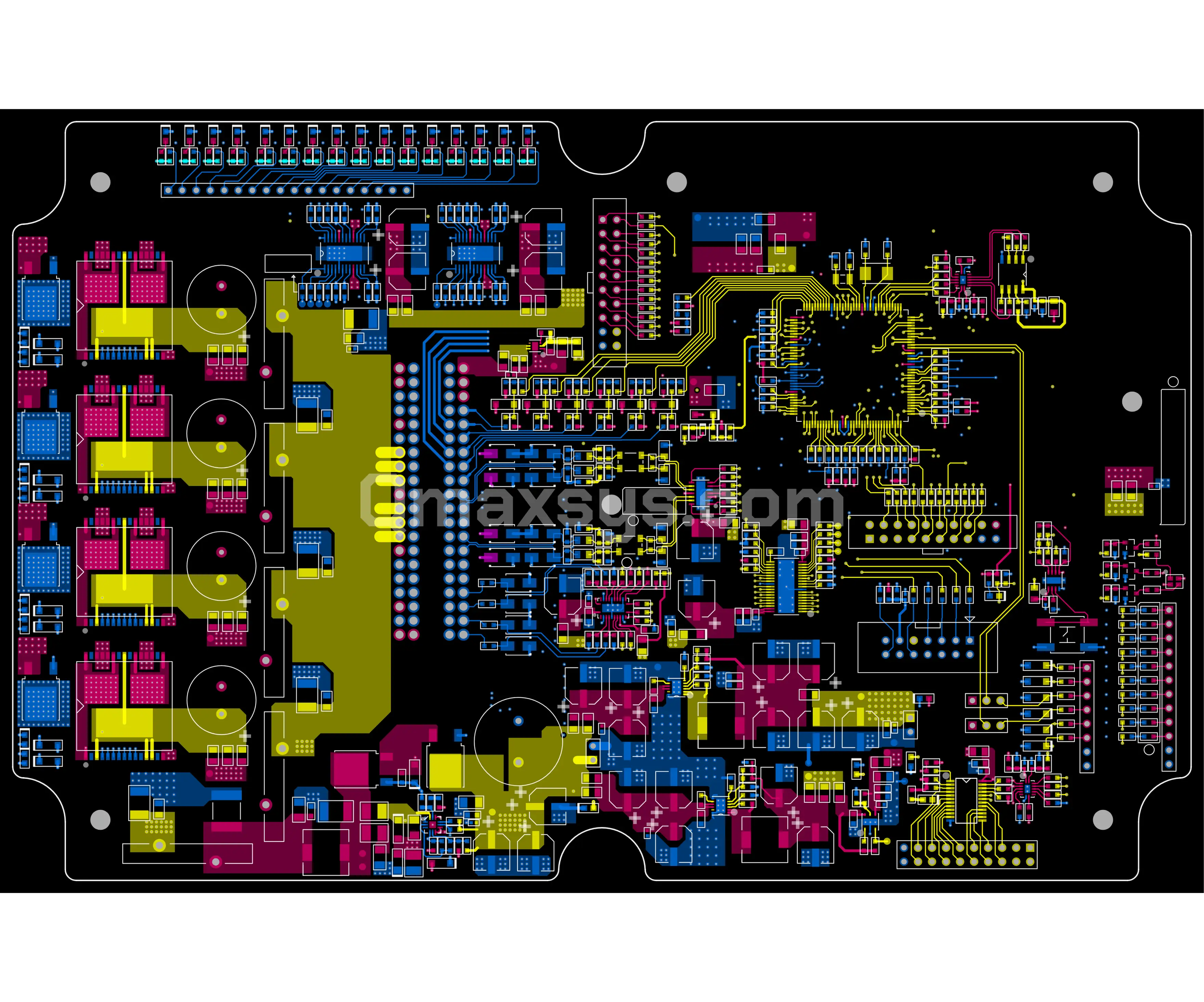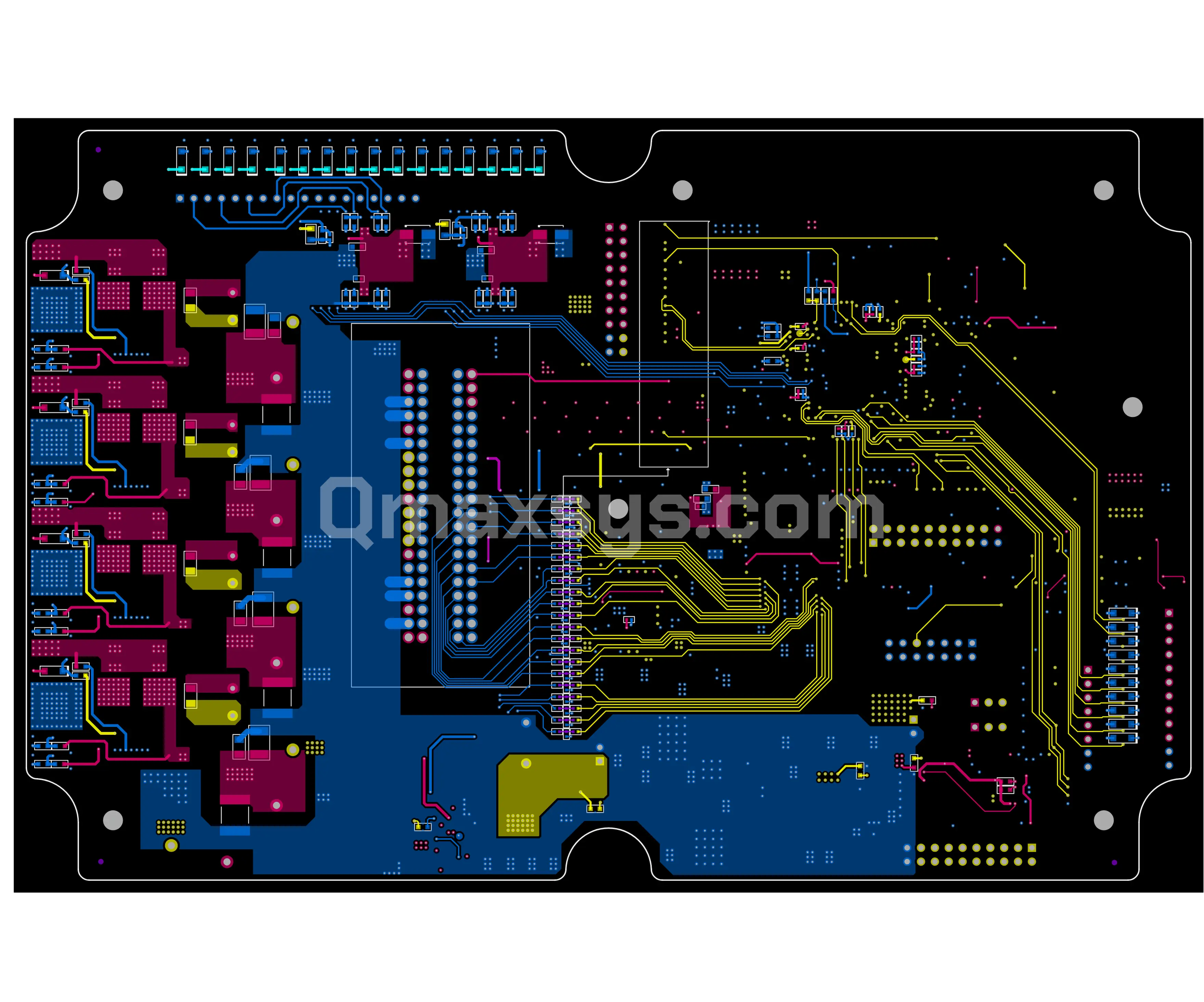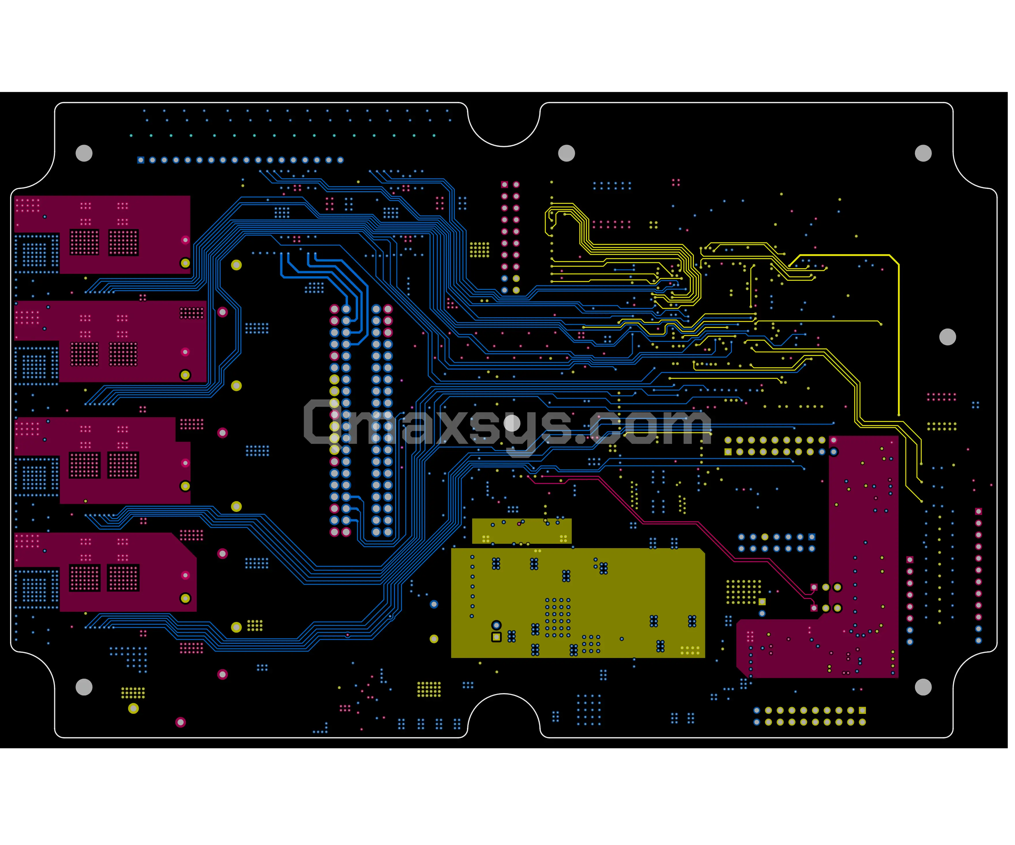
PCB Design Services Engineering for First-Time-Right Hardware

TALK TO OUR ENGINEERS

PCB Lifecycle

From Requirement to Production

Qmax Systems provides PCB design services that treat the board as a critical engineering discipline, not mere interconnection. Qmax Systems delivers reliable, first-time-right PCB layouts, validated by SI/PI and thermal simulation for performance, compliance, and manufacturability.

Requirement Capture
Schematics
Netlist / BoM
Mechanical Drawing
Application specific constraints
Library Development
Footprint creation
Footprint review
Design Environment Setup
Define board outline
Set mechanical constraints
Set physical / electrical constraints
Set up stackup
Component Placement
Component placement
Placement review
PCB Routing
Power routing
Signal routing
Power plane creation
Length matching
SI / PI / Thermal Analysis
Pre-route analysis
Post-route SI analysis
Thermal Analysis
Design Verification
DRC / ERC Check
DFM Review
Manufacturing Review
Final Design Sign-off
Manufacturing Outputs
Silkscreen Editing
Assembly Drawing
Fabrication Drawing
Generate Gerbers

PCB Design Capabilities

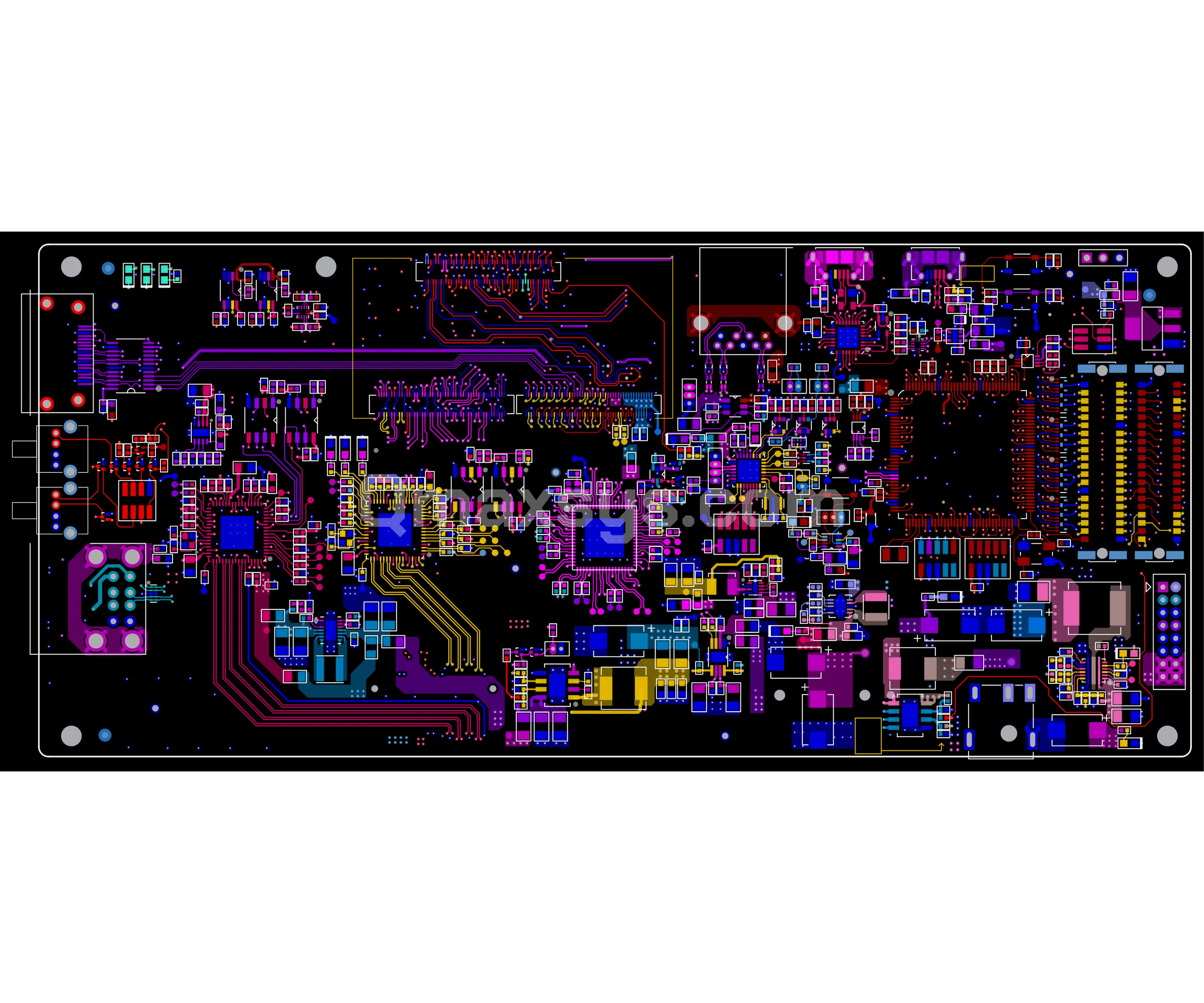
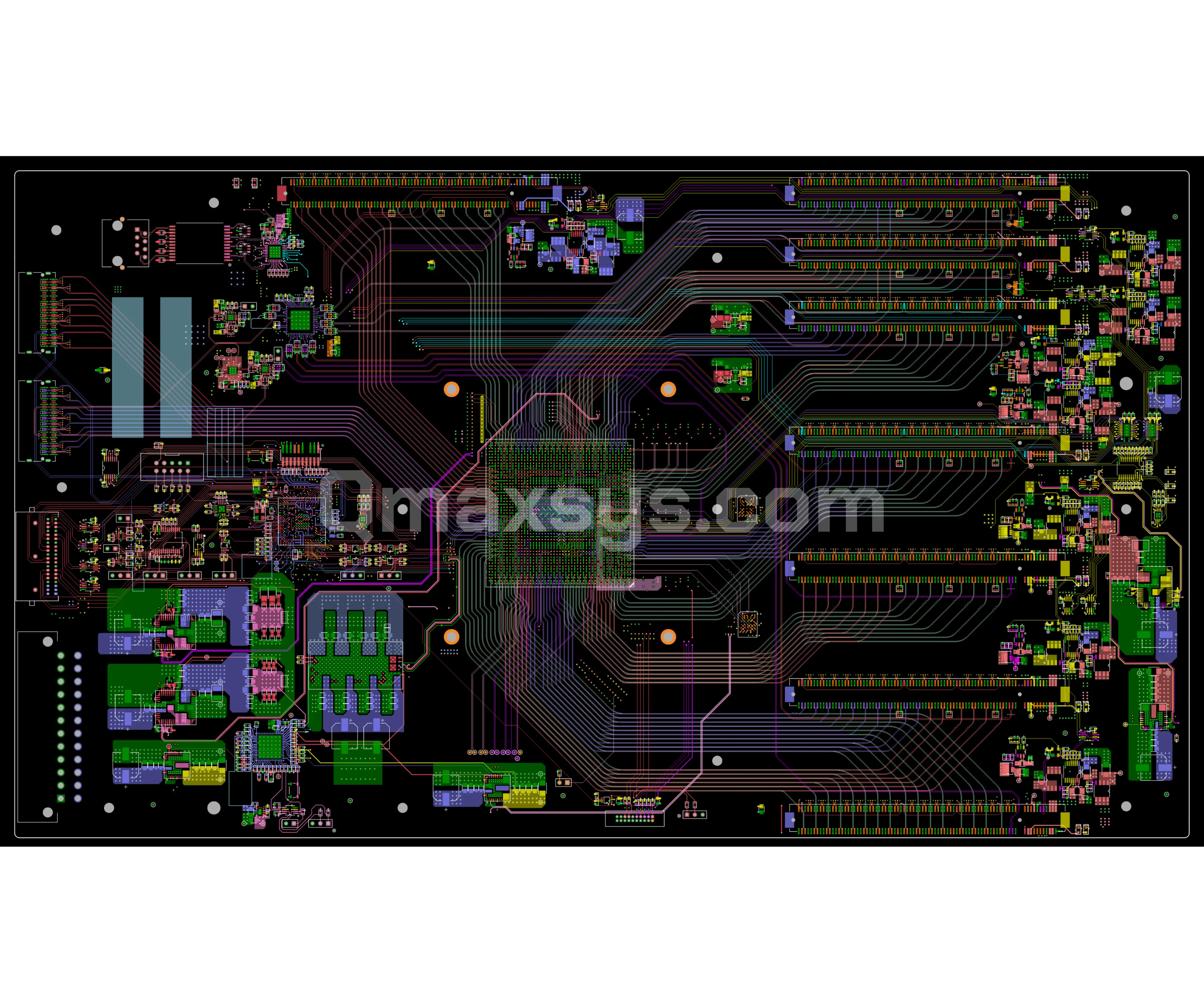
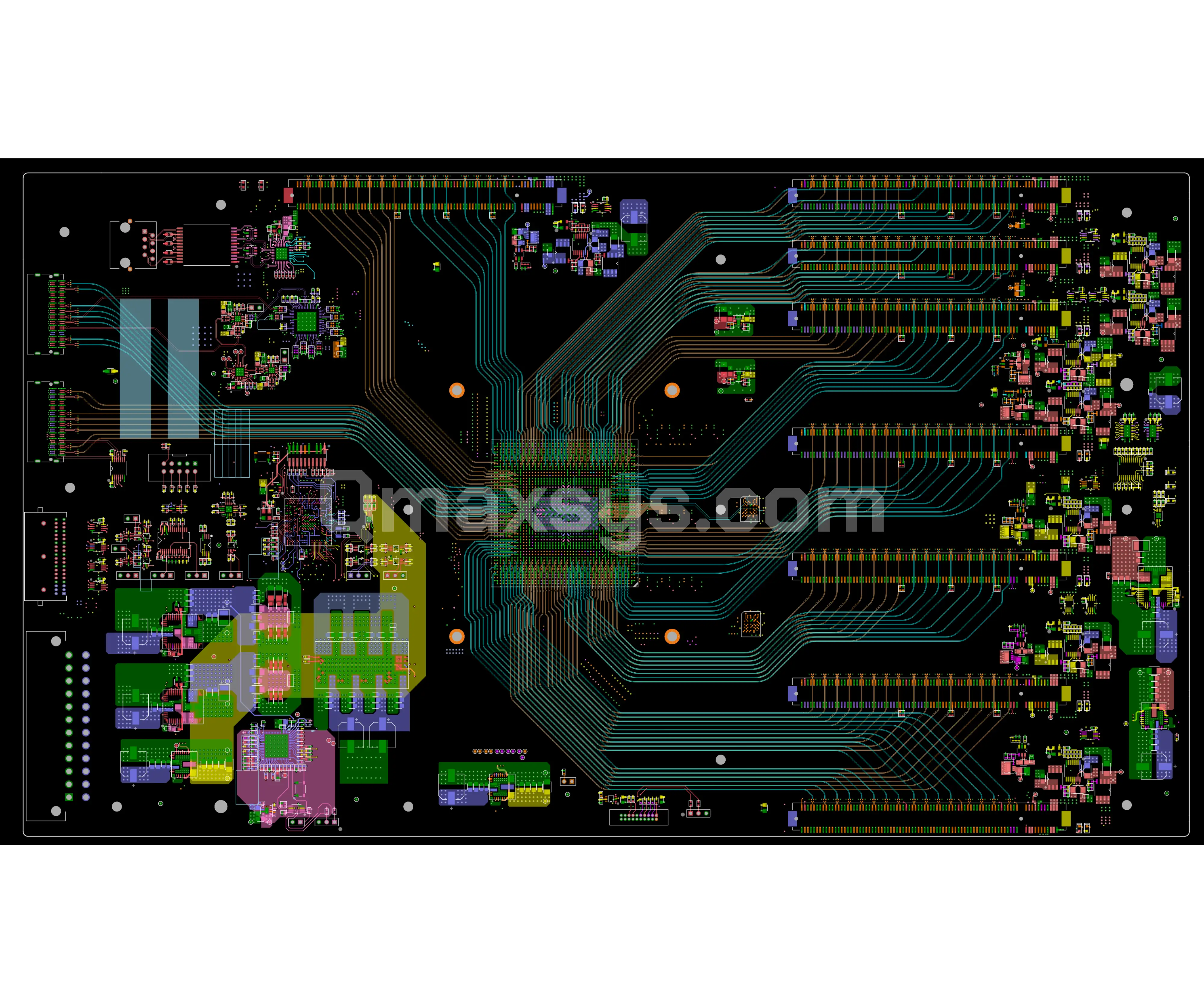
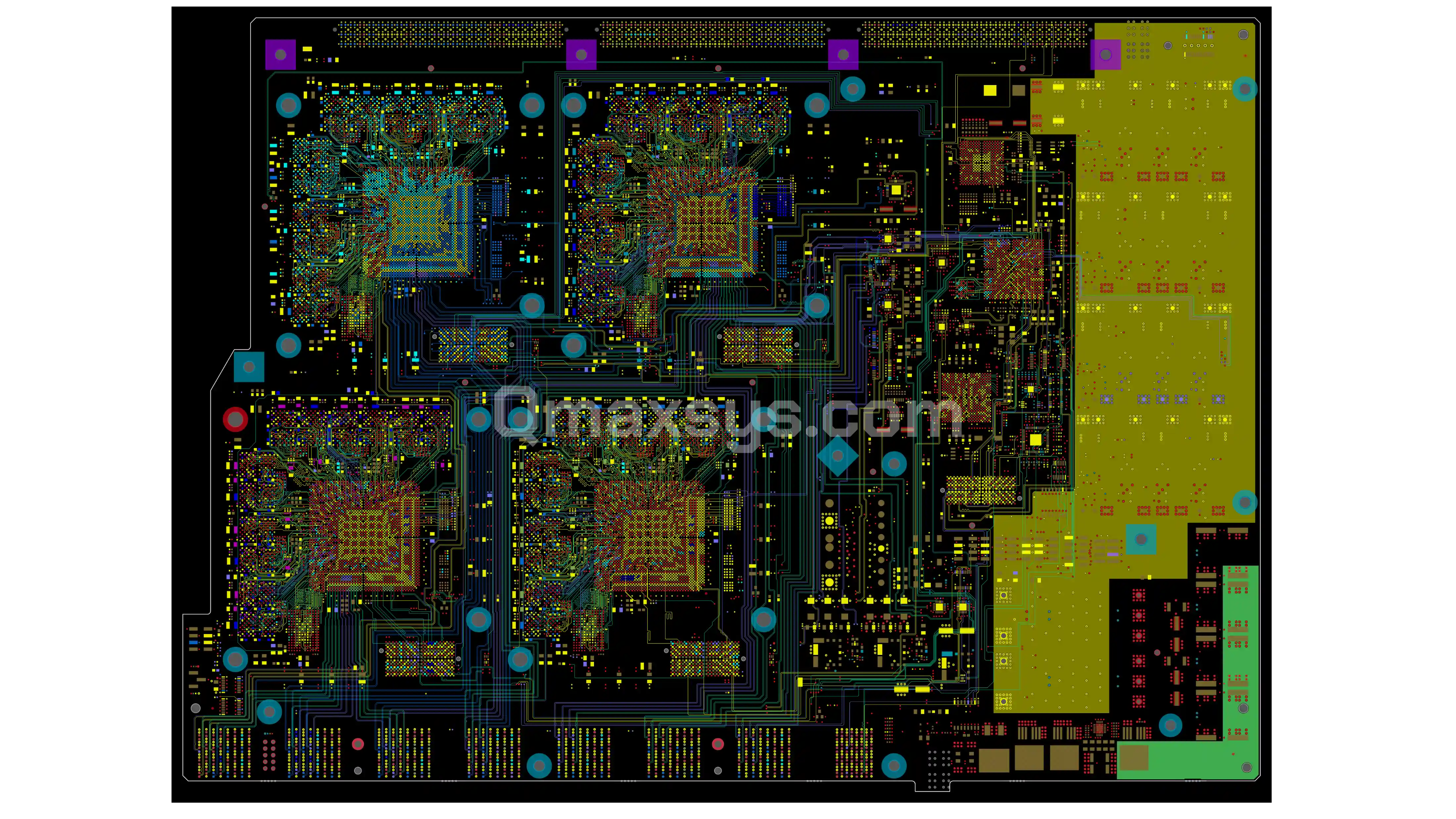
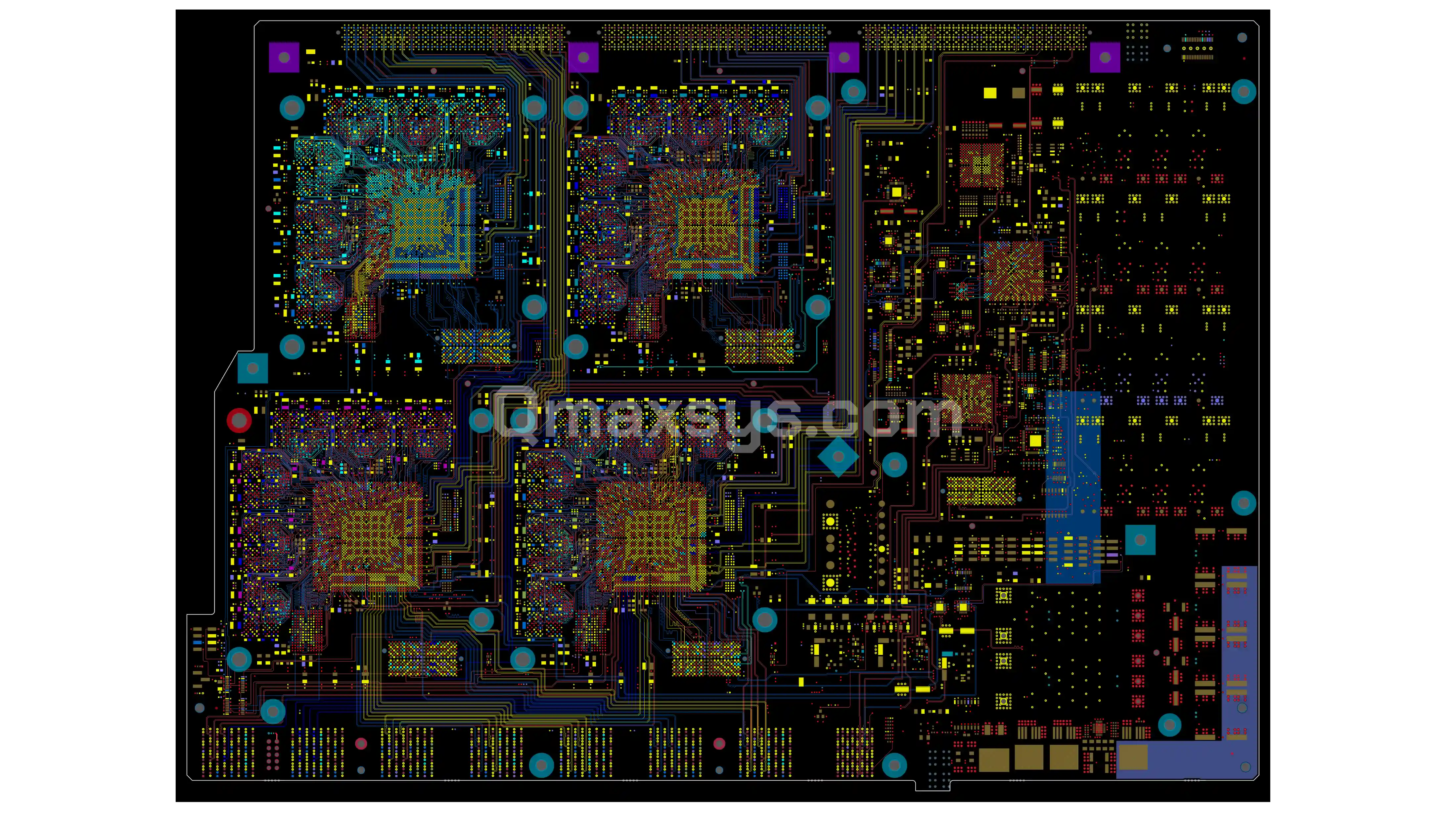
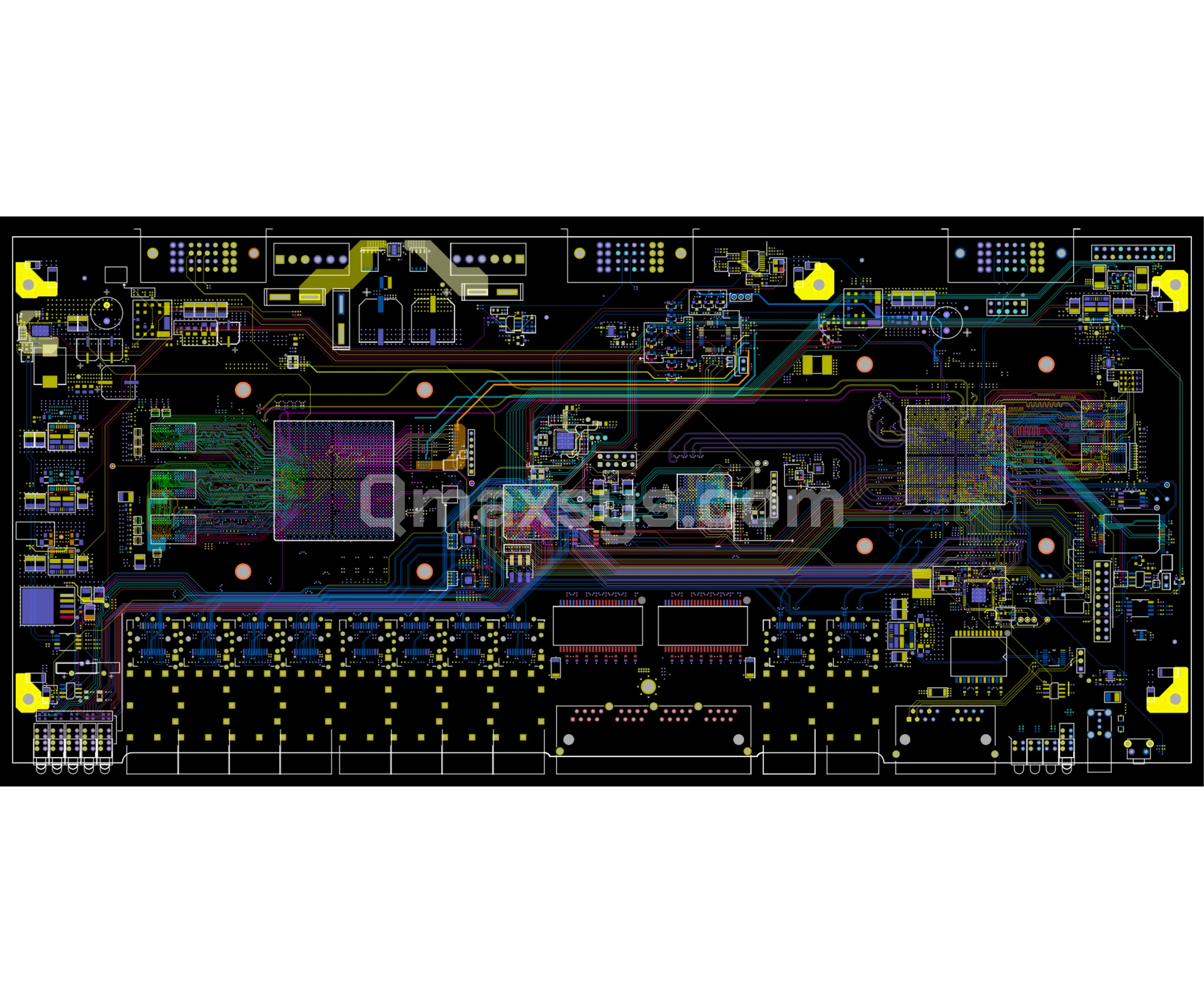
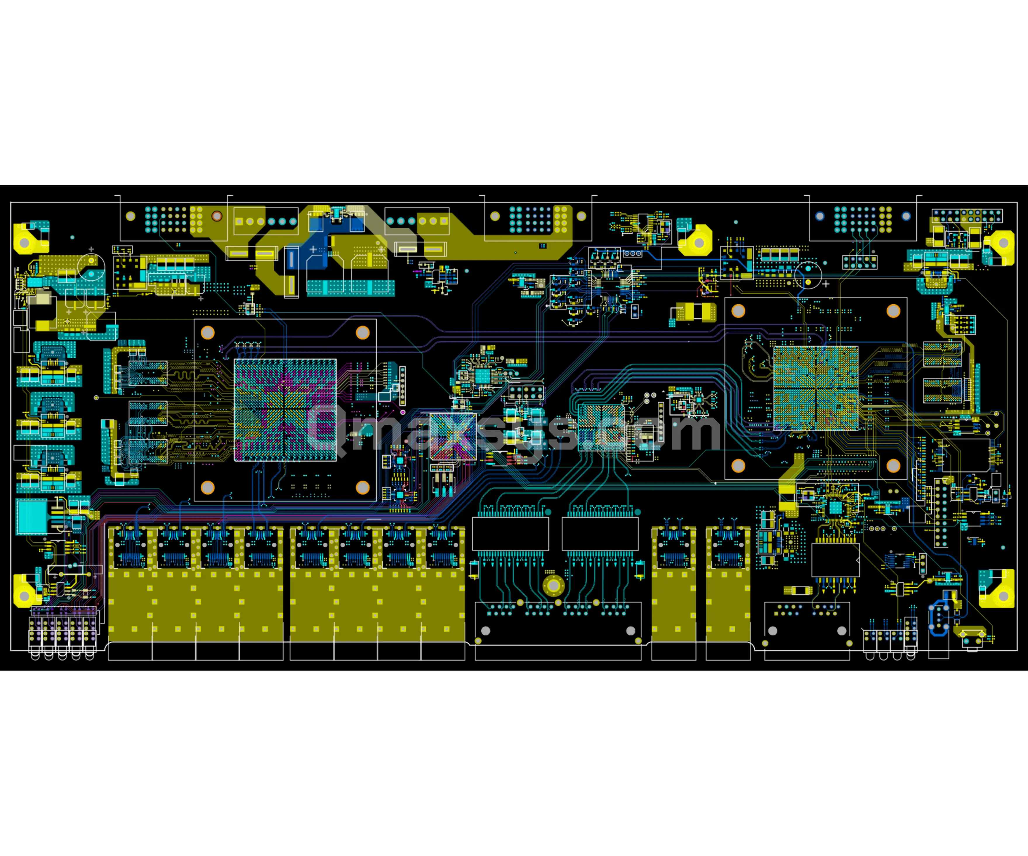
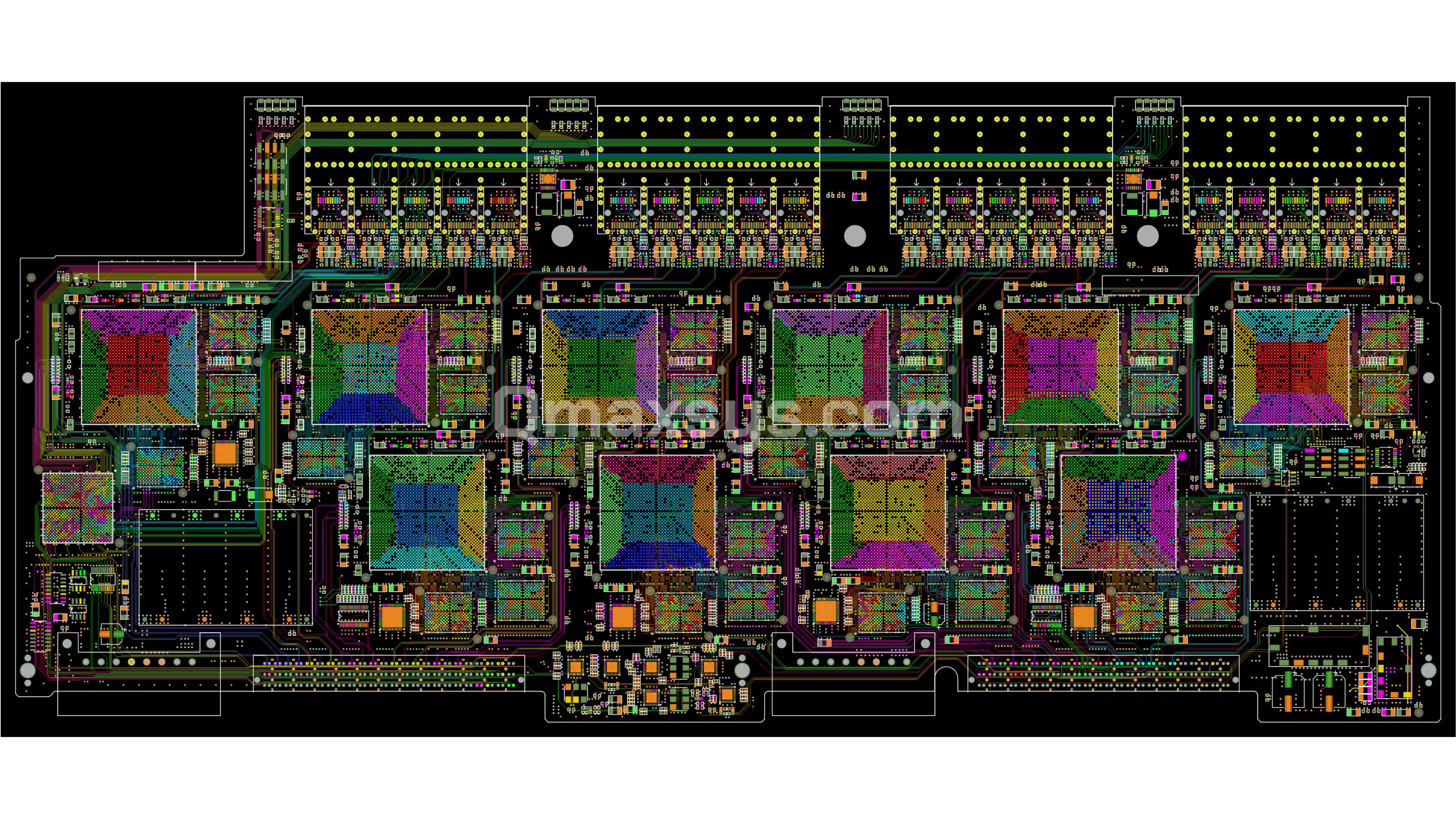
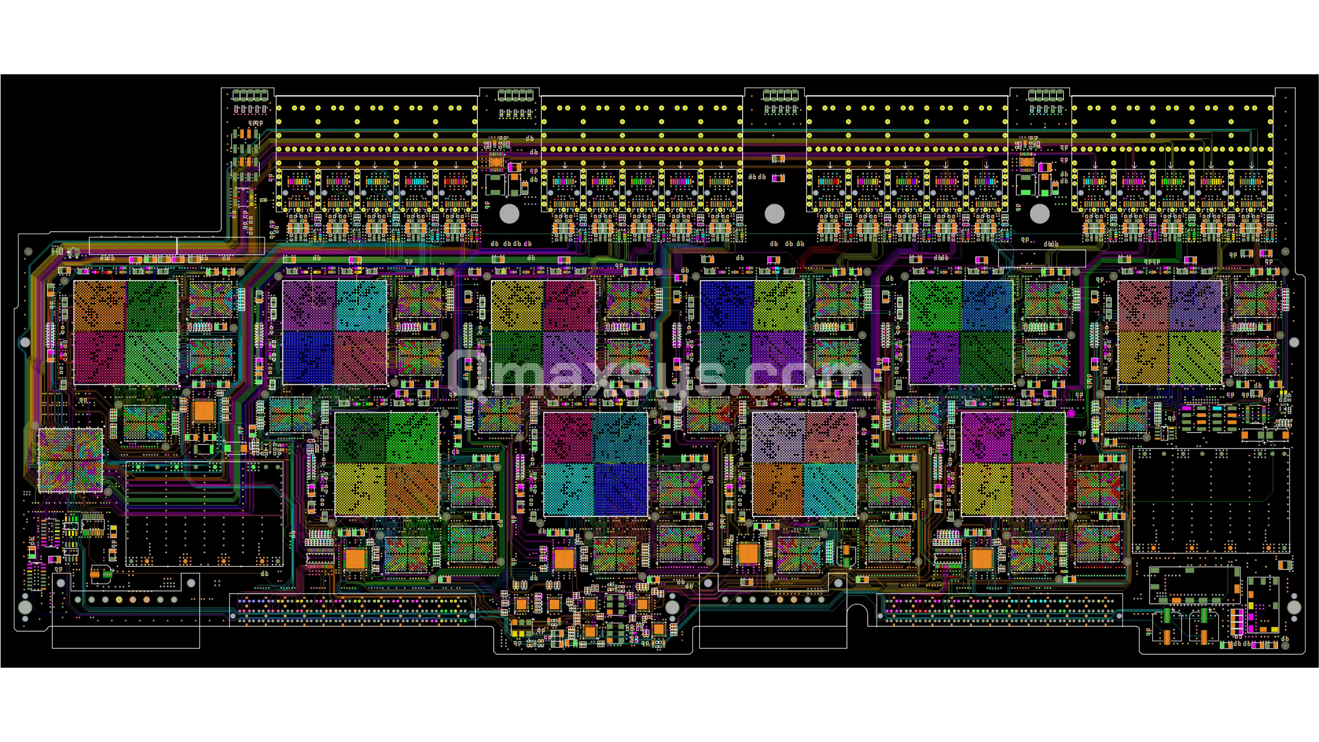
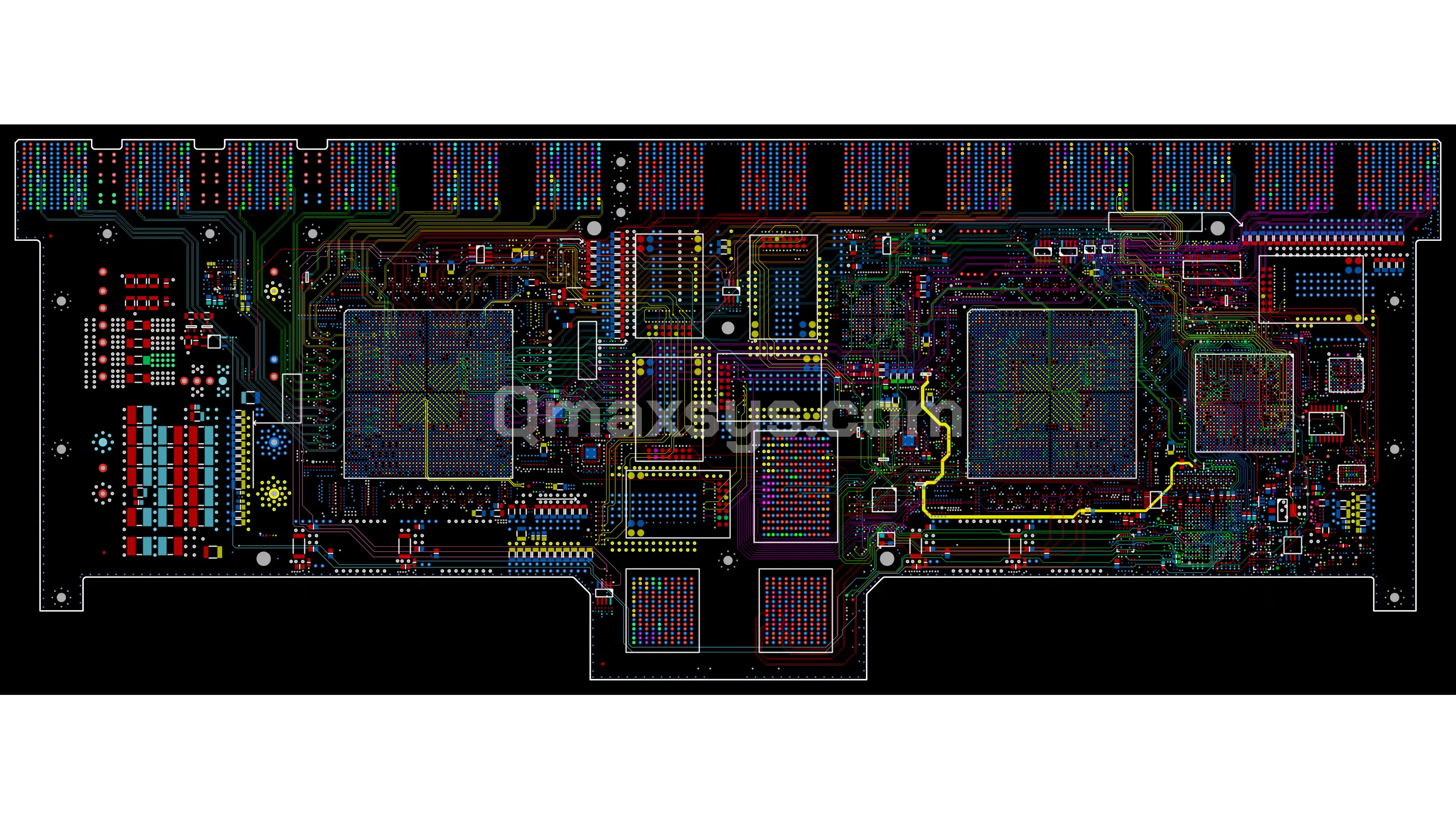
High-density AI GPU chassis motherboard PCB

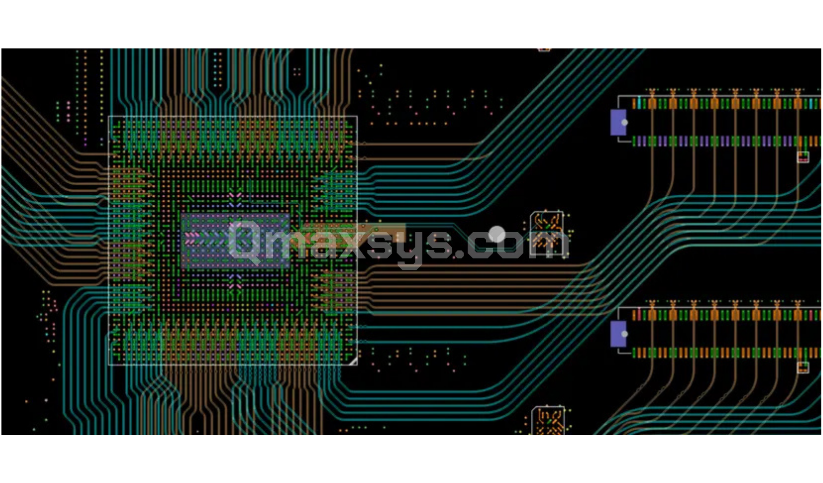
High-Speed PCB Design

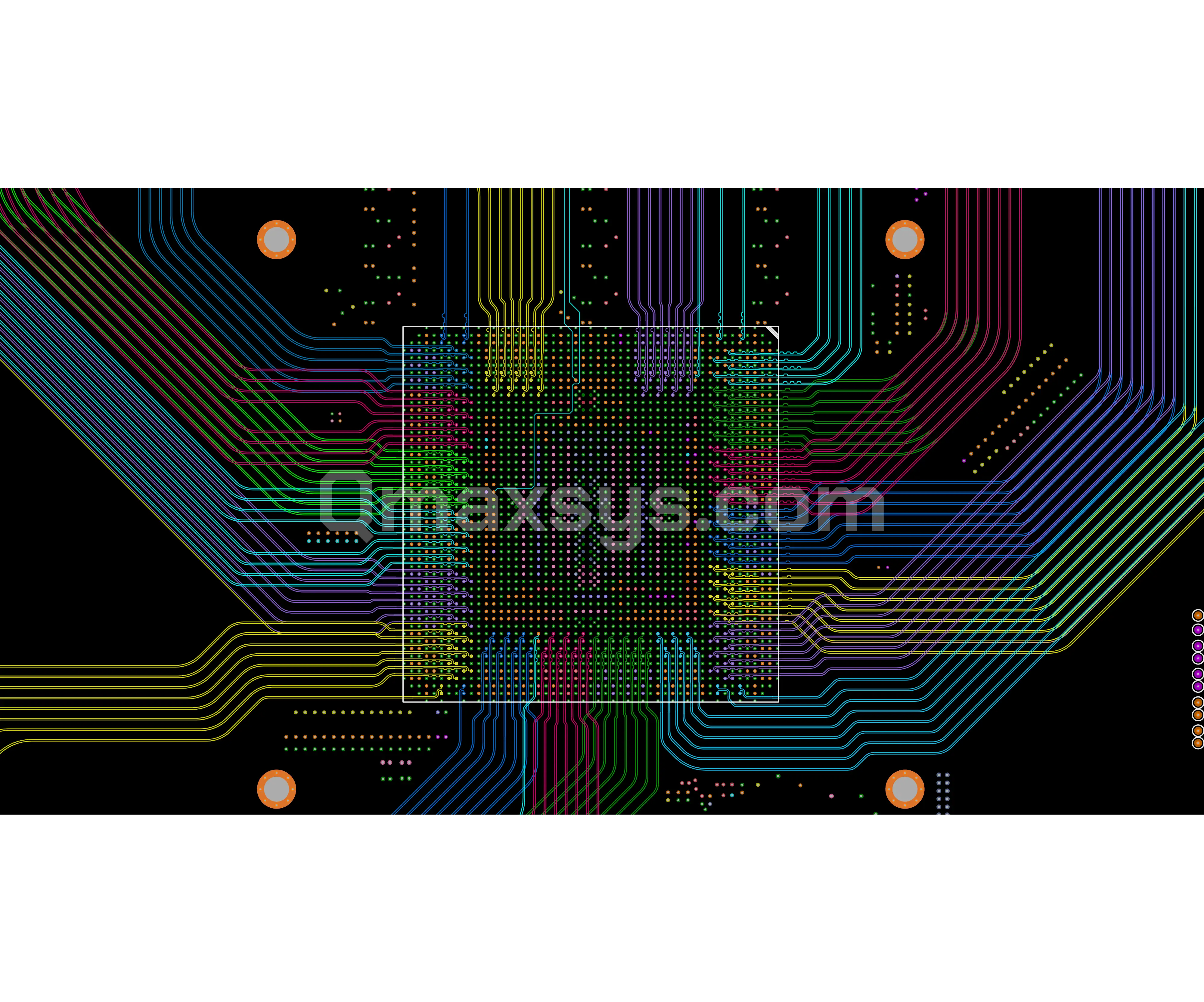
DDR4/DDR5, PCIe Gen3/Gen4, and 10/25G SerDes lanes validated through pre- and post-layout SI/PI simulation. Applications: server compute, networking line cards, FPGA boards.

  • Standards & Interfaces: IPC-2221, IPC-2152, IPC-2141 controlled-impedance routing; DDR3/4/5, PCIe Gen3/4, 10G/25G SerDes, USB 3.x, HDMI.
  • Tools & Verification: Cadence Sigrity, Ansys SIwave for SI/PI simulation; length-matched differential pairs, return-path integrity, decap optimization.
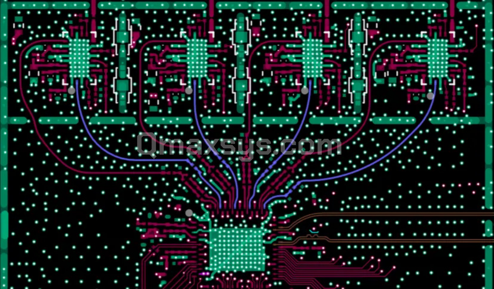
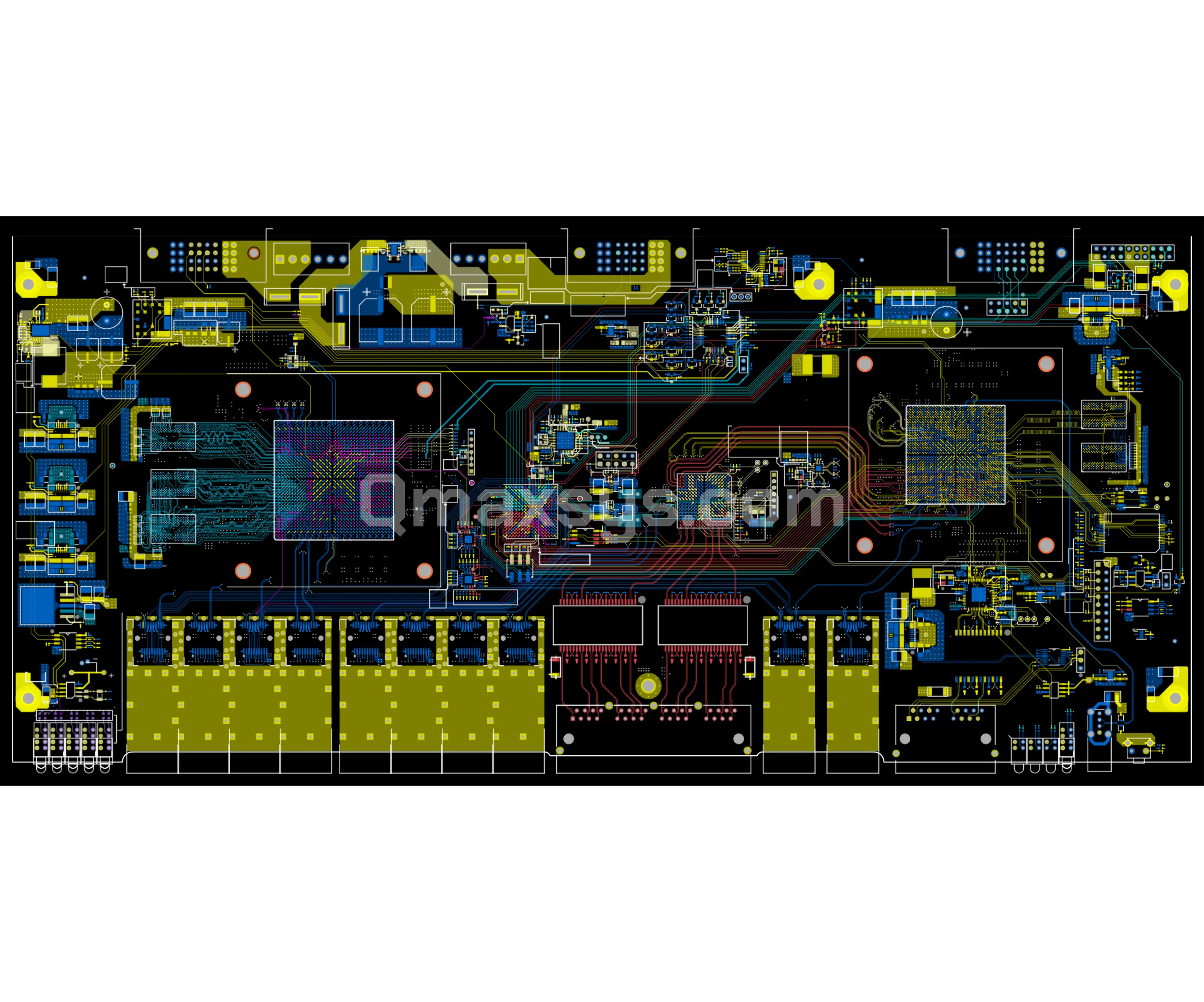
Qualcomm Wi-Fi 6 triband router PCB

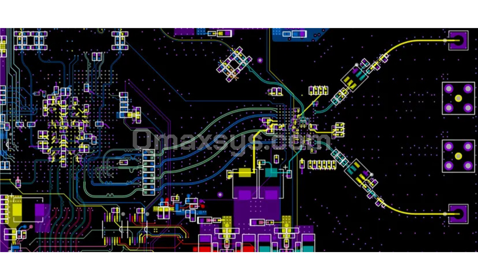
RF & Microwave PCB Design

Front-end architecture, antenna integration, and EMC-aware layout qualified across ISM, Wi-Fi, BLE, LTE, and Sub-GHz bands. Applications: IoT radios, industrial telemetry, wireless medical devices.

  • Components & Antennas: RF front-end design (LNA, PA, filters, matching networks); PCB, external, horn, and custom antenna integration.
  • Protocols & Validation: ISM, Wi-Fi, BLE, LTE, and Sub-GHz systems; RF simulation, tuning, calibration, and EMC-aware layout.
High-speed analog mixed-signal PCB

Analog & Mixed-Signal PCB Design

Low-noise sensor interfaces, ADC/DAC conditioning chains, and EMI-hardened layout integrated into a single qualified board. Applications: biomedical instrumentation, industrial sensing, optical acquisition.

  • Sensing & Front-Ends: Low-noise analog front-ends and sensor interfacing; pressure, vibration, biomedical, and optical signal acquisition.
  • Processing & Integrity: Signal conditioning, filtering, amplification, ADC/DAC integration; EMI-aware analog layout and grounding techniques.
Safron power electronics PCB

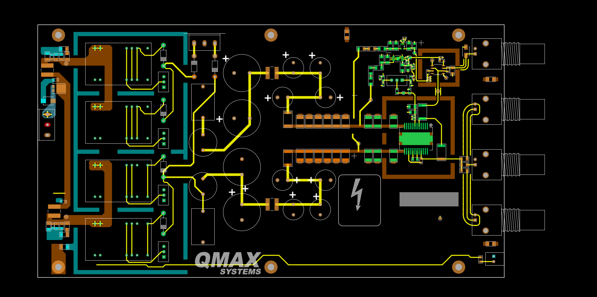
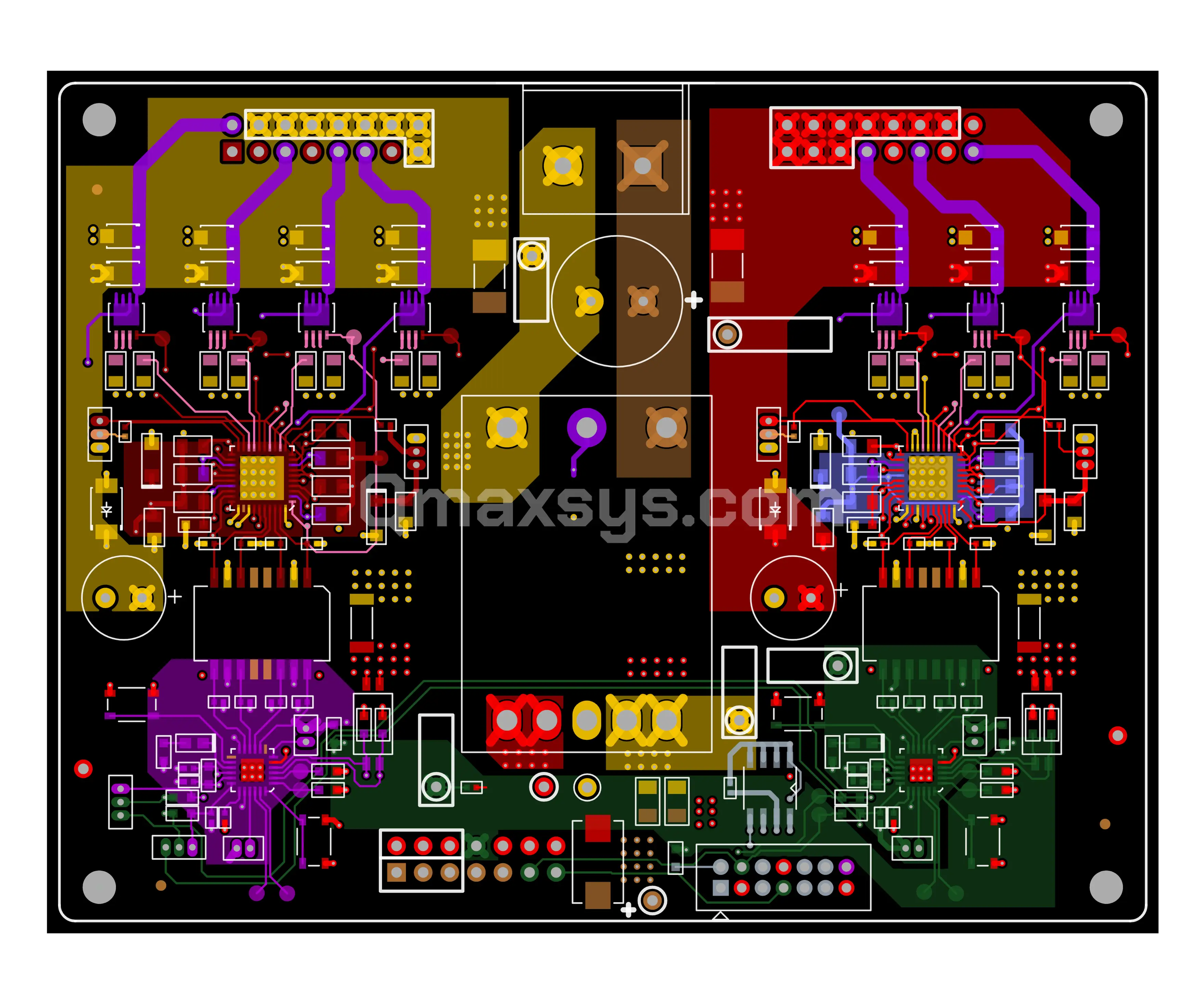
Power Electronics PCB Design

AC-DC and DC-DC converters, BMS, and HV/HC PCBs verified against derating and reliability targets. Applications: EV charging, industrial drives, grid-tied energy storage.

  • Conversion & Topologies: AC-DC/DC-DC converters and isolated/non-isolated SMPS; resonant, LLC, CLLC, and Class-D topologies.
  • High Power & Reliability: Battery systems (BMS), chargers, inverters, HV/HC PCB design; thermal simulation, derating, and reliability analysis.
Signal and power integrity analysis

SI / PI Analysis

Cadence Sigrity and Ansys SIwave for transmission-line simulation, eye-diagram analysis, IBIS modeling, and PDN impedance — standalone or integrated into any layout engagement. Applications: DDR5, PCIe Gen4/5, SerDes channels.

  • Simulation & Modeling: Transmission line simulation, eye diagram, and IBIS-based driver/receiver modeling.
  • PDN & Decoupling: Power delivery network impedance analysis and decoupling capacitor optimization.
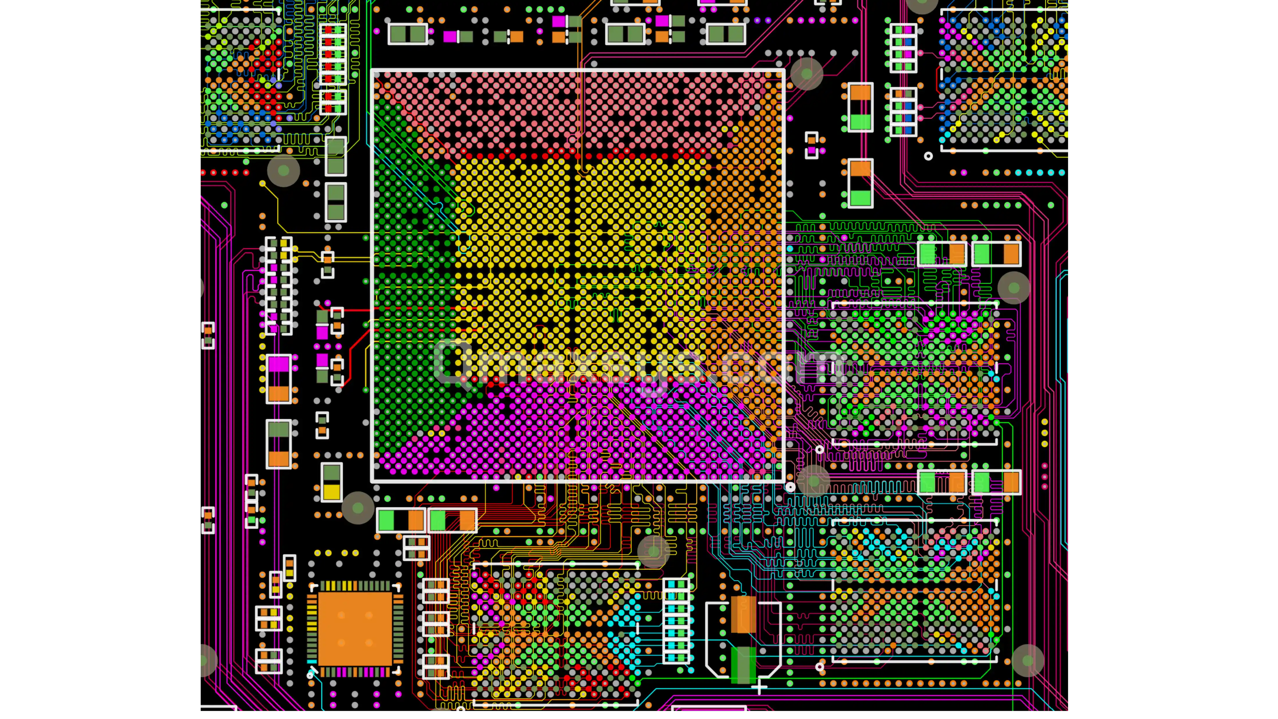
PCB design review checklist

PCB Design Review

Independent audit of your existing layout covering stack-up, placement, routing, silkscreen, drill notes, and documentation. Deliverable: formal technical report with prioritized SI, DFM, thermal, and compliance findings.

  • Review Coverage: Stack-up, placement, routing, silkscreen, drill notes, and documentation completeness.
  • Deliverable: Formal technical report with prioritized SI, DFM, thermal, and compliance findings.

PCB Design Across Industries

Designing printed circuit boards for mission-critical applications requires strict adherence to industry-specific compliance, signal integrity, and environmental standards. At Qmax Systems, our engineering team brings over 29 years of specialized expertise in layout design, stackup optimization, and high-reliability routing across regulated sectors. We integrate Design for Manufacturability (DFM), Design for Assembly (DFA), and Design for Testing (DFT) directly into the layout workflow, ensuring full compliance from day one. Whether handling high-speed differential pairs, high-voltage creepage requirements, or severe thermal loads, our industry-focused PCB design services turn complex system architectures into production-ready, fully compliant hardware.

Aerospace & Defense

Our aerospace design capabilities focus on high-reliability, ruggedized PCB layouts built to withstand extreme shock, vibration, and thermal stress. We strictly adhere to IPC-2221 Class 3 guidelines, DO-160 environmental standards, and MIL-STD-461 EMI specifications, incorporating thermal vias, thick copper weights, and tight clearance rules for harsh operational environments.

Qmax has delivered defense-grade PCB designs for complex systems, including Software Defined Radios (SDR), high-speed data acquisition systems, structural health monitoring hardware, cable tension meters, and dual-redundant joystick controllers for eVTOL aircraft.

Aerospace & Defense PCB design

Why Choose Qmax for PCB Design?

First-Time-Right Philosophy

Before Gerbers leave the building, Qmax Systems runs DRC, SI/PI, and thermal simulation, setting routing constraints up front so the first fabricated board behaves as designed - no costly re-spins.

Zero-Defect Design Assurance

Backed by 29 years of expertise and hundreds of complex PCB layouts, Qmax enforces a zero-defect engineering culture. Every high-speed, high-density, or high-power layout undergoes strict peer reviews using checklists perfected over three decades—guaranteeing defect-free design handoffs every time.

Global Compliance Expertise

CE, FCC, UL, IPC, and MIL-STD-461 are designed in at the layout stage, because Qmax Systems treats compliance as a confirmation, not a gamble - via an EMC-by-design approach.

30,000+ Verified Component Libraries

Qmax Systems validates every symbol, footprint, and 3D model against manufacturer datasheets across 30,000+ verified components — eliminating pad mismatches and assembly surprises.

Production & Documentation Readiness

Every design ships with 100% DFM-verified files to IPC-2221/2226; Qmax Systems delivers complete IPC-2581/ODB++ packages, controlled-impedance drill tables, and worst-case tolerance analysis.

Strict IP Protection

A mutual NDA is signed from day one, and Qmax Systems stores all design files in an access-controlled vault, never on shared drives: Customers own all IP at every milestone.

Frequently Asked Questions

Does Qmax Systems provide end-to-end PCB design services?
Yes. Qmax Systems handles the full PCB design cycle - from schematic capture and stack-up planning to detailed layout, signal integrity analysis, and Gerber generation. IPC-trained designers manage every step from initial netlist to fabrication-ready output, giving you one accountable team for every PCB your product depends on.
What PCB technologies and complexities does Qmax Systems handle?
We design everything from 2-layer boards to 32+ layer HDI, rigid-flex, and mixed-signal PCBs. Qmax Systems routinely delivers high-density BGA fanouts, controlled-impedance routing, blind and buried vias, and length-tuned high-speed channels - every layout engineered for performance, manufacturability, and reliable operation across demanding environments.
Which PCB design CAD tools does Qmax Systems support?
Qmax Systems is proficient across all major PCB CAD platforms, including Altium Designer, Cadence Allegro, Mentor Xpedition, OrCAD, KiCad, and PADS. We adapt to your existing toolchain and library standards, ensuring seamless collaboration with your in-house engineering teams and full design-data compatibility from start to finish.
Does Qmax Systems handle high-speed and signal integrity design?
Yes. Our high-speed expertise covers DDR4/DDR5, PCIe Gen5, USB 4.0, Ethernet up to 112G SerDes, and RF up to mmWave. Qmax Systems runs pre-layout and post-layout SI/PI/EMI simulations in Cadence Sigrity and Ansys SIwave, and manages crosstalk, return paths, and power integrity across every critical net.
Does Qmax Systems perform DFM and pre-fabrication reviews?
Yes. Qmax Systems runs every design through internal DFM, DFA, and DFT reviews before fabrication release, and coordinates directly with your manufacturing partners on stack-up, panelization, and tolerance to identify yield risks early. The result is a manufacture-ready design package that minimizes spins, reduces NRE, and shortens time to volume.
How does Qmax Systems protect our PCB design data and IP?
Every engagement operates under strict NDAs with employees, customers, and third-party vendors. Qmax Systems stores design files on access-controlled, encrypted servers with role-based permissions and complete audit trails. You retain 100% IP ownership, and your schematics, layouts, and libraries are never reused, shared, or referenced beyond your project.
Contact Us