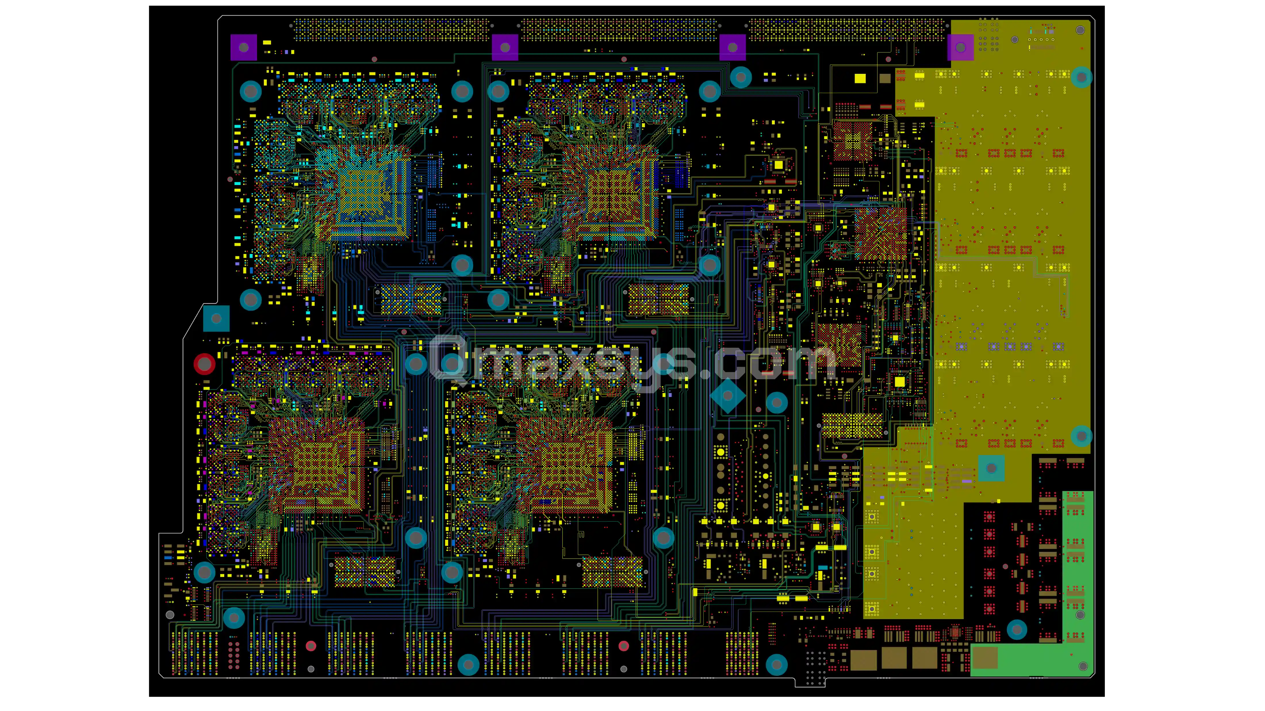
Copper Cannot Be Wide, Tight and Far Apart at the Same Time
Qmax Systems has laid out power electronics boards since 1997 — 29 years of heavy-copper stack-up definition, busbar integration, creepage and clearance geometry, switching-loop and gate-loop minimization, thermal path design, and fabricator alignment on builds most shops will not quote. The team are Electrical and Electronics Engineers with IPC CID certification — necessary here, because a clearance table is only useful to someone who understands what the working voltage is doing to the air around it.
A power board is a functional circuit element, not interconnect. The copper is a conductor with a temperature rise, an inductance and a thermal spreading path all at once, and those three requirements pull against each other. Widen the pour for current and the loop area grows. Tighten the loop for di/dt and the clearance shrinks. Add clearance for the working voltage and the board grows. Nothing in that trade-off is visible on a schematic, and all of it is decided in the stack-up and the placement.
Delivered work covers copper weights from 4 oz to 14 oz, power planes and integrated busbar structures carrying more than 1000 A of DC, board-level isolation designed to 1500 VDC working voltage, and boards for a 3 kV / 100 A power module, a 300 kW SiC inverter and a 45 kVA rack PDU shipped in the hundreds and certified to UL489 and UL1077.
Copper weight to 14 oz per IPC-4562, cross-section sized for temperature rise per IPC-2152
Creepage & Clearance
Spacing from working voltage, pollution degree, altitude and CTI, before placement
Busbar Integration
Embedded and laminated busbar structures, terminations, current collectors
Switching Loop Layout
Gate loop and power loop inductance minimized, DC-bus caps coupled tight to devices
Thermal Path Design
Thermal via arrays, IMS and metal core, copper spreading tracked to simulation
EMI Containment
Loop area control at source, CM choke, Pi-filter and snubber placement
Verification & Release
DRC and ERC, DFM, DFA and DFT review, Gerber or IPC-2581 package
Power Electronics Boards We Design
High-Current Distribution and Busbar Boards
Boards whose job is to move current without a hot spot. Copper cross-section, parallel-device current sharing and the mechanical interface to a busbar are the whole design, and a symmetry error shows up as one device running hotter than its neighbors.
Heavy copper stack-ups from 4 oz to 14 oz per IPC-4562
Embedded and laminated busbar structures with low loop inductance
Symmetric routing for balanced current sharing across parallel devices
Busbar-to-board mechanical and electrical termination design
Conductor sizing for temperature rise per IPC-2152, not from ampacity tables alone
High-Voltage Isolation Boards
Boards where the spacing table drives the floor plan. At 1500 VDC the distances required are not distances that can be found late, so creepage and clearance are computed first and used as placement constraints.
Clearance and creepage to IEC 60664-1, cross-checked against IPC-2221
Slot cuts, routed channels and reinforced isolation zones
Pollution degree, altitude derating and CTI-driven material selection
Primary-to-secondary barrier definition with no copper, via or plane bridging
Board-level isolation designed to 1500 VDC working voltage
Battery, BMS and Energy Storage Boards
The physical power path around a bought-in stack controller: getting current out of the cells, into the busbar, and through a safety envelope that holds at pack voltage. Sense wiring has to run alongside all of it without corrupting its own measurement.
Cell interconnect and current-collector design
Laminated busbar stacks with insulation coordination at pack voltage
Voltage and temperature sense flex PCBs alongside high-current paths
Contactor, pre-charge, fusing and insulation-monitoring layout
Cell balancer boards, active and passive
Converter and Inverter Boards
Switching stages where the gate loop and the power loop decide whether the design meets its efficiency number and its emissions limit. With wide-bandgap devices the edge rate that delivers the efficiency is the same edge rate that causes the trouble.
SiC and GaN power stages with minimized gate-loop inductance
Isolated gate driver boards with high common-mode transient immunity
Resonant LLC and CLLC, PSFB, bridgeless totem-pole PFC and multiphase interleaved layout
Three-phase inverter power stages and DC-bus capacitor placement
Bidirectional converter layout at kilovolt class
Metering, Protection and Distribution Boards
Boards that measure and switch mains power, where the metering has to stay accurate while sitting against the switching it is measuring, and where the protection has to isolate a fault without taking down its neighbors.
Three-phase distribution boards with per-outlet switching and metering
Polyphase metering front-end layout calibrated to approximately 1% accuracy
Breaker, fuse and protective device layout with coordinated discrimination
Mains-isolated multi-board architectures with barrier signaling
UL489 and UL1077 assemblies taken through certification
Thermal-Critical and Encapsulated Boards
Boards where the heat has to leave through the board rather than off a component, and boards that have to survive an environment with nothing to do with their electrical function.
Thermal via arrays under power devices to heatsink or chassis
IMS and metal-core substrates for direct-to-chassis heat paths
Copper-embedded construction for extreme current density or spreading
Epoxy-encapsulated automotive assemblies qualified for vibration and temperature
Custom heat sink and cold plate interface definition
Board Complexity We Design To
Parameter
What we design to
Boards we have designed
Layer count
2 to 36 layers available; power stages usually land between 2 and 6, thick rather than deep
3 layers carrying the 45 kVA PDU output stage — one heavy layer shaping the mains current, two thinner layers for control and sensing
Routing and plane budget
A uniform plane is often the wrong use of a layer; high current wants a shaped pour sized for its own temperature rise
3 routing layers with no dedicated plane on the PDU power board, verified from the design database
Copper weight
4 oz to 14 oz per IPC-4562, cross-section derived from allowable temperature rise per IPC-2152
Power planes and integrated busbar structures carrying more than 1000 A of DC
Working voltage
Board-level creepage and clearance from IEC 60664-1 and IPC-2221 against working voltage, pollution degree and altitude
Board-level isolation designed to 1500 VDC; boards for a 3 kV / 100 A SiC power module and a 1500 V / 400 kW bidirectional converter
Spacing and geometry
Minimum spacing set by the voltage, not by the partner's etch floor — slot cuts and routed channels where distance cannot be found
Reinforced isolation zones and routed barriers on mains and HV assemblies, with no copper, via or plane permitted to bridge them
Drill and via structures
Through-hole with thermal via arrays placed for heat transfer rather than for connectivity
125 through-vias on the PDU power board — a low count on purpose, because on a high-current board every via is a thermal and mechanical decision
Board thickness
Chosen for copper build-up and mechanical strength under busbar termination loads
63 mils on the PDU power board, with a 10 mil minimum drill, read from the design database
Interconnect
Embedded and laminated busbar structures, current collectors, busbar-to-board terminations
A laminated busbar taken through six concept iterations to freeze for a 1000 V DC pack, plus its cell current collector and sense flex
Thermal construction
Thermal via arrays, IMS and metal core, copper-embedded builds where current density or spreading is extreme
Custom heat-sink interfaces on a 90 A marine drive; epoxy-encapsulated automotive assembly at 10,000-unit volume
Base materials
FR-4 and high-Tg per IPC-4101, insulated metal substrate where the die must dump heat into the chassis
High-Tg where ambient is elevated; IMS where the thermal path had to leave through the board rather than off a component
Performance class
IPC-6012 Class 2 or Class 3, plus UL 796 bare-board recognition on UL 94 V-0 laminate
UL489 and UL1077 certified PDU boards specified to IPC-6012 Class 2 or Class 3
Applications & Real-World Project Experience
Power integrity and grounding optimization for a PCIe Gen 5 AI GPU expansion chassis motherboard, with a multi-rail power-delivery plane, hot-swap 12 V inputs, and target-impedance PDN design that sustains high-current GPU loads alongside high-speed fabric signaling.
Automotive power and load-driving layout for an EV VCU demo platform, with multi-rail regulation, dual-channel H-bridge motor drive, 16-channel high-side switching, and load-dump / reverse-polarity protection across vehicle power inputs.
SMPS and power-converter layout for a modular medical simulator, implementing a high-power PoE backbone and multiple regulated conversion rails that deliver both data and actuation power to each manikin module over a single Ethernet cable.
Multi-rail power distribution and high-side switch drive layout for a 240-channel industrial I/O controller, with protected power stages and isolated domains supporting continuous factory-floor operation across five synchronized MCUs.
Current capacity is not a table lookup. The cross-section a conductor needs depends on the allowable temperature rise, the ambient, the copper weight, whether the conductor is internal or external and what is spreading heat around it — which is why IPC-2152 replaced the old charts. Qmax sizes conductors from the permitted rise and then checks the built board with thermal imaging.
Copper weight 4 oz to 14 oz specified per IPC-4562
Cross-section derived from allowable temperature rise per IPC-2152
Power planes and busbar structures carrying more than 1000 A of DC
Symmetric routing so parallel devices share current rather than fight over it
Etch compensation and manufacturability agreed with the fabricator for heavy copper
Clearance Computed Before Placement
Creepage and clearance are derived from working voltage, overvoltage category, pollution degree, altitude and material CTI, then used as placement constraints. Treated as a final check instead, they force a re-layout — because the distances a 1500 VDC board needs are not distances that can be found late.
Spacing derived per IEC 60664-1 and cross-checked against IPC-2221
Altitude derating applied where the product ships above 2,000 m
Pollution degree assessed from the real enclosure, not assumed benign
Slot cuts and routed channels where distance alone cannot be found
Barrier keep-outs enforced on every layer, with no via or plane bridging
Two Loops, Both Small
A switching stage has a power loop and a gate loop, and both have to be small. The power loop area sets the radiated emissions and the voltage overshoot; the gate loop inductance sets the ringing and, with wide-bandgap devices, whether the gate stays under control at all. Shrinking them is geometry, done at placement.
DC-bus capacitors coupled tight to the switching devices to shrink the hot loop
Gate-source loop inductance minimized in copper, not compensated in firmware
Kelvin source connections where the device package offers them
CM chokes, Pi-filters and snubbers placed at the source of the disturbance
Emissions designed against CISPR 32, CISPR 11 and CISPR 25 as applicable
Requirement
Standards basis
What it constrains in the layout
Printed board design and fabrication
IPC-2221, IPC-2152, IPC-4562, IPC-6012 Class 2 or 3, UL 796, UL 94 V-0
Board-level voltage spacing, conductor cross-section for current, copper foil weight, board performance class, and UL recognition of the bare board
Insulation coordination
IEC 60664-1
Clearance, creepage and solid insulation against working voltage, overvoltage category, pollution degree and altitude — this is what sets component pitch
Power conversion equipment
IEC 62477-1, IPC-9592
Protective separation in converter systems, and design, qualification and reliability requirements for power conversion devices
Drive systems
IEC 61800-5-1
Electrical, thermal and energy safety for power drive systems
IT and network equipment
IEC and UL 62368-1
Hazard-based safety for IT and communication equipment. Replaced UL 60950-1, which is withdrawn
Breakers and protective devices
UL 489, UL 1077, EN 60934, IEC 60947-2
Molded-case breakers, supplementary protectors, appliance couplers and low-voltage switchgear
Battery energy storage
IEC 62619, IEC 63056, UL 1973, UL 9540A
Cell and system safety for industrial lithium batteries and stationary storage
Automotive and e-mobility
ISO 26262, AEC-Q100 and Q101, CISPR 25, UN ECE R10, AIS 004 Part 3
Functional safety, component qualification, and component-level automotive EMC, certified through ARAI in India
Medical power
IEC 60601-1 with IEC 60601-1-2
Cited only where the product is a medical device. It is not a general high-voltage isolation basis and should never be used as one
How a Power Board Gets From Netlist to Release
The Expensive Errors Are Physical
A power board rarely fails because of a logic mistake. It fails because a pour was sized from an ampacity chart instead of a temperature rise, because a clearance passed on the PCB and was then bridged by a harness, or because a gate loop was left large enough to ring the device into destruction.
Stage-gate checklists, each with a named owner and a recorded outcome
In-house scripts auditing conductor cross-section, spacing and switching-loop geometry
Every check names its authority: IPC-2221 for board spacing, IPC-2152 for conductor sizing, IPC-4562 for copper weight, IPC-6012 for performance class, IPC-A-600 and IPC-A-610 with J-STD-001 for acceptability, IPC-2231 for design-for-excellence — because on a mains board "it looked fine" is not a defense
Release Is Read Aloud by Two People
One engineer reads the item, a second confirms the state out loud — a flight-crew checklist, deliberately. On a mains or HV board the stakes make it non-negotiable: the item nobody wants to re-read at release is the isolation barrier, and that is precisely the one that has to be spoken and confirmed.
Challenge and response on every release item, spoken and confirmed
Copper weight, spacing table and slot geometry cross-read against the working voltage
Isolation barriers confirmed unbridged on every layer, including the assembly view
Sign-off recorded against a name, not just a date
What Lands in Your Hands
A release package that carries the physical requirements a power board depends on, not just its copper geometry. You own all of it.
Gerber and drill data, or IPC-2581 (DPMX) and ODB++
Fabrication drawing with copper weight, slot cuts and isolation call-outs
Assembly drawing with creepage keep-outs, potting boundaries and torque-critical hardware noted
BoM, netlist and IPC-D-356 bare-board test data
Loss budget and thermal analysis records against the operating points
Native CAD source files in the tool the design was built in
Stage
What it means on this kind of board
What has to be true before it closes
1Requirement Capture
Working voltage, continuous and peak currents per path, ambient, allowable temperature rise, and whether the assembly is potted
The insulation requirement and the thermal budget are both numbers, agreed, before anything is drawn
2Library Development
High-current pad geometry, thermal relief that does not defeat the thermal path, creepage-aware footprints
Land patterns conform to IPC-7351 and BGA practice to IPC-7095, and no footprint quietly violates the spacing the voltage demands
3Design Environment Setup
Copper weight chosen, spacing table computed from voltage and pollution degree, thermal targets set
The spacing table exists and is a placement constraint — not a rule to be checked against later
4Component Placement
Spacing drives component pitch, the switching loop is planned, the thermal path is planned
The isolation barrier is a straight, unbroken region, and the hot loop is already small
5PCB Routing
Shaped pours sized for temperature rise, gate loops kept tight, sense taken as Kelvin pairs
Current sharing between parallel devices is symmetric, not left to luck
6Loss and Thermal Analysis
Loss budget per operating point, thermal simulation, protection coordination curves compared across levels
Predicted junction temperatures are inside derating at the real ambient, not at 25 °C
7Design Verification
DRC and ERC, 3D clearance on the full assembly including harness and brackets, DFM and DFA with the partner
Clearance holds in three dimensions, not merely in copper — a bracket can violate what the PCB passed
A partner who has never built this product can still build it safely
Why Choose Qmax for Power Electronics PCB Design
Boards Some Shops Will Not Quote
Copper from 4 oz to 14 oz, power planes and busbar structures carrying more than 1000 A of DC, isolation to 1500 VDC, IMS and copper-embedded construction. These builds need a partner with real process capability behind them, and they need a specification written in terms that partner can actually hold — which is the part most design houses get wrong.
Certification Behind the Numbers
A power claim is worth what the certificate behind it is worth. Boards laid out by Qmax are UL489 and UL1077 certified on a 45 kVA PDU shipped in the hundreds to US data centers, ARAI certified on a 10,000-unit automotive program, and UL certified on a patented product built in the tens of thousands.
Heat Designed In, Not Bolted On
A loss budget per operating point comes first; thermal simulation then drives via arrays, pour shapes and the heat-sink interface; and the built board is thermally imaged against that model. When the image and the model disagree, that is a finding to investigate — not a surprise to absorb after the product ships.
Engineers Who Know What the Voltage Is Doing
Power layout is one discipline inside a broader first-time-right PCB design practice. A spacing table is only useful to somebody who understands why it says what it says. Every Qmax PCB designer is an Electrical or Electronics Engineer, and the team holds IPC CID certification — awarded by IPC rather than claimed in a brochure.
Routed to a Partner With the Process
Qmax works with verified fabrication partners across the United States, Japan, South Korea, Taiwan and India. For heavy copper, routed isolation slots and metal-core construction the choice of shop is a technical decision rather than a commercial one, and it is made before layout begins.
ISO 9001 and ISO 13485, and 100% Your IP
Design work runs inside certified quality systems with the document control and traceability that medical and regulated programs require. A mutual NDA precedes any technical discussion, files are held under role-based access rather than on shared drives, and you own every schematic, layout, library and simulation file at every milestone. Qmax retains no rights and reuses nothing across clients.
Get a Complimentary Consultation with Our Power Electronics PCB Experts
A one-hour session with a senior Qmax PCB design engineer. Bring a schematic, a current path and a working voltage, or a board running hotter than it should. You will get a view on which physical constraint is actually binding — not a proposal.
What copper weight and current can Qmax Systems design to?
Copper weights from 4 oz to 14 oz, specified per IPC-4562, with power planes and integrated busbar structures carrying more than 1000 A of DC. Conductor cross-section is derived from the allowable temperature rise using IPC-2152 rather than from legacy ampacity charts, because the current a conductor can carry depends on the permitted rise, the ambient, the copper weight, whether the conductor is internal or external, and what is spreading heat around it. Heavy copper also changes what the fabricator can hold, so etch compensation and manufacturability are agreed with the shop before release.
What voltage class does Qmax Systems lay out to?
Board-level isolation is designed to 1500 VDC working voltage, and Qmax has laid out boards for a 3 kV / 100 A power module and a 1500 V / 400 kW bidirectional converter. Clearance and creepage are derived per IEC 60664-1 from the actual working voltage, overvoltage category, pollution degree and altitude, and cross-checked against IPC-2221 board spacing. Those distances are then used as placement constraints, because at these voltages the spacing table drives the floor plan rather than being checked against it.
Why is creepage and clearance computed before placement rather than checked afterwards?
Because the distances cannot be found late. At 1500 VDC in a polluted environment at altitude, the required spacing between primary and secondary is a large fraction of the available board area, and a layout that ignored it until DRC has to be substantially re-done rather than adjusted. Computing it first turns it into a constraint the floor plan is built around: component pitch, barrier position, slot cuts and routed channels are all decided at once. Verification then runs in 3D on the assembly model as well as on the PCB, because a clearance that passes in copper can be violated by a harness, a bracket or a fastener.
How does Qmax Systems lay out SiC and GaN switching stages?
By making both loops small. The power loop — DC-bus capacitor, switch, return — sets the radiated emissions and the voltage overshoot, so the bus capacitors are coupled tight to the devices to shrink the enclosed area. The gate loop sets the ringing, and with wide-bandgap devices it determines whether the gate stays under control at all, so gate-source inductance is minimized in copper and a Kelvin source connection is used where the package offers one. The same edge rate that delivers the efficiency couples into the current-sense path and anything sharing a reference, so those are separated deliberately. This was the core of the work on a 300 kW SiC traction inverter gate driver.
Can a 3-layer board be the right answer?
Yes, and the 45 kVA PDU power board is the proof: 3 routing layers with no dedicated plane, carrying 415 VAC three-phase at 45 kVA across 41.68 square inches with 100% routing completion and zero DRC errors in the released database. On a heavy-copper board a plane is often the wrong use of a layer, because high current wants a shaped pour sized for its own temperature rise rather than a uniform sheet. One thick layer carries the mains current while two thinner layers carry relay control and sensing. Odd layer counts are unusual, but unusual is not the same as wrong.
How does Qmax Systems get heat out of a power board?
By designing the thermal path as part of the layout rather than bolting a heatsink on afterwards. Thermal via arrays are placed under power devices for heat transfer rather than for connectivity — which is why via count on a power board is low and deliberate. Where the die has to dump heat straight into the chassis, IMS or metal-core construction is used; where current density or spreading is extreme, copper-embedded construction. Copper pours and stack-up are tracked to thermal simulation results, and the built board is then thermally imaged against that model so a discrepancy becomes a finding rather than a surprise.
Does Qmax Systems design busbar-to-board integration?
Yes, and it is one of the distinguishing capabilities. Work includes embedded and laminated busbar structures forming low-inductance current paths, the mechanical and electrical termination between a busbar and the board, and cell current collectors on battery programs. On a 1000 V DC-class grid storage pack Qmax designed the laminated busbar through six concept iterations before freeze, plus the current collector and the sense flex PCB. A separate 3 kV / 100 A power module uses proprietary copper busbar technology developed for that program.
How do you keep sense wiring accurate next to a high-current path?
By partitioning and by geometry, the same discipline the analog page describes. Sense conductors are routed away from the switching loop and never parallel to it for any length; sense returns are taken to a single defined point rather than to the nearest copper; shunt connections are made as Kelvin pairs so the measurement does not include the voltage drop across the joint; and where the sense path has to cross a domain, it crosses once at a controlled bridge. On a battery pack the voltage and temperature sense flex has to run the length of a 1000 V current path and still resolve millivolts, and that is achieved by routing discipline and per-tap protection rather than by filtering.
How does Qmax Systems keep power boards inside emissions limits?
By containing the disturbance at its source. Loop area is minimized first, because a small loop radiates less than a filtered large one; slew rate is controlled where the design can afford it; common-mode chokes, Pi-filters and snubbers are placed at the disturbance rather than at the connector; and every conductor that leaves the board is treated as an antenna and filtered where it crosses the shield boundary. Designs are worked against CISPR 32 for IT equipment, CISPR 11 for ISM, and CISPR 25 with UN ECE R10 for automotive. Where a board has already failed, near-field probing locates the source before anything is changed.
Can Qmax Systems take over a power board that is running hot or failing emissions?
Yes, and both are common engagements. Thermal failures are diagnosed by comparing a measured thermal map against a rebuilt loss budget, which usually shows one loss term was underestimated — switching loss at the real dead time, core loss at the real flux density, or conductor loss at the real current density with the real copper weight. Emissions failures are traced to the power loop, then the common-mode path, then the cable crossing the boundary, in that order. In both cases the deliverable is a diagnosis with measurement behind it and costed options, which is often a re-layout of one region rather than a new board.
What is different about laying out an encapsulated board?
The board stops being in air. Once potted, heat leaves by conduction through the compound rather than by convection off components, so the thermal model changes completely and hot spots move. Component height and the potting boundary become keep-out constraints, tall parts have to be positioned so the compound flows around them without voiding, and the coefficient of thermal expansion mismatch between compound and board puts mechanical stress on joints through every temperature cycle. The bus kneeling and leveling controller is epoxy encapsulated and was qualified for EMI, vibration and temperature before ARAI certification at 10,000-unit volume.
Does Qmax Systems handle metering and protection layout?
Yes. On the 45 kVA PDU the metering board holds roughly 1% accuracy across 30 outlets from five ST STPM34 front-ends while sandwiched against the power board carrying thirty switching relays — achieved with per-channel calibration stored in flash rather than by filtering. Protection layout covers breaker and fuse placement with coordinated discrimination across main, branch and load levels, so the device closest to a fault is the one that operates. Assemblies have been taken through UL489 and UL1077 certification with Qmax managing the program.
Which fabricators can build these boards?
Not all of them, and that is the point. Heavy copper needs a shop that can hold etch compensation on thick foil; 1500 VDC spacing needs one that can hold routed slot tolerances; IMS and copper-embedded builds need specific process capability; and a 3-layer heavy-copper board is an unusual request that some shops will simply decline. Qmax works with several of the world's leading fabricators, agrees stack-up and process capability before layout opens rather than at quotation, and will work with your preferred shop provided the build is genuinely within their process.
Can Qmax Systems lay out our power board from our schematics?
Yes, and most power engagements start that way. A schematic review runs first, because on a power board the schematic often hides the layout problem — a current-sense return taken from the wrong node, a gate resistor placed where its loop cannot be small, or an isolation barrier crossed by a signal nobody noticed. Work is delivered in Altium Designer, Cadence Allegro and OrCAD, Siemens Xpedition and PADS, Zuken or KiCad, and native source files are handed back in the tool the design was built in.
What information does Qmax Systems need to quote a power layout?
Schematics or a netlist, the mechanical outline, the BoM, and then the four things that size the job: the working voltage and therefore the insulation requirement, the continuous and peak currents in each path, the ambient and the allowable temperature rise, and the markets the product ships into. Whether the assembly is potted matters too, because that changes the thermal design. If the loss budget does not exist yet, Qmax builds it as a first deliverable. An NDA is signed before any technical discussion.