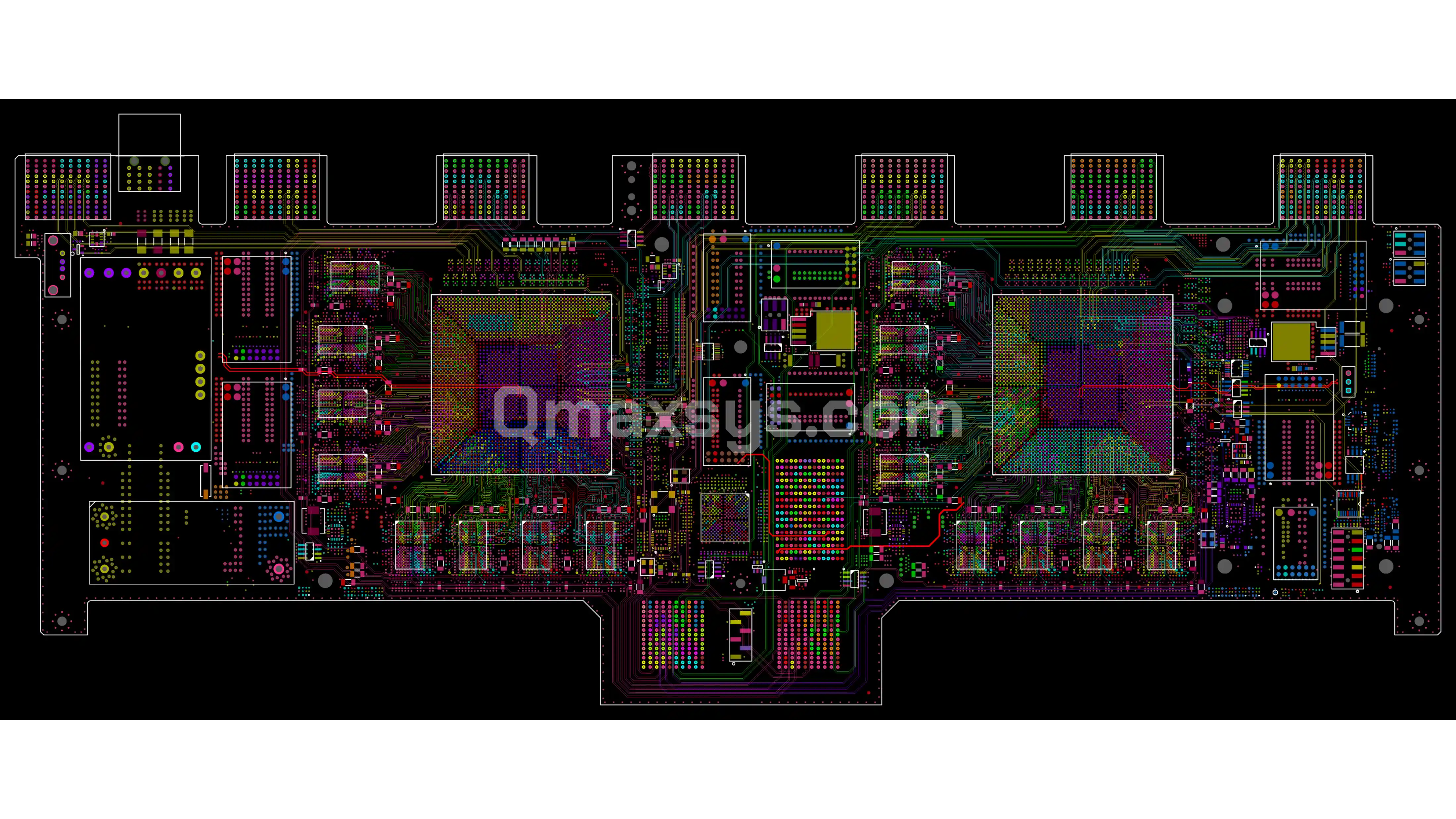
High-Capacity Packet-Processing Line Card
Project Overview
Qmax Systems was engaged by a Canadian networking equipment company to execute the full physical PCB design of a high-capacity packet-processing line card built around dual Broadcom BCM88650 (Arad) network processors. The customer supplied verified schematics and a complete design-input package; Qmax owned the layout of a 36-layer, controlled-impedance, carrier-grade AdvancedTCA (ATCA) blade. The card performs packet classification, deep-buffer traffic management, and cell-based fabric interfacing, connecting to a companion switch-fabric card over the chassis backplane. High-speed SerDes routing, a 32-device DDR3 memory array, and power integrity made this one of the most demanding boards in the platform.
Application Brief
The board is a line/packet-processing blade inside a modular ATCA-based packet-optical transport platform used by service providers for metro and core Carrier Ethernet / MPLS aggregation. Two BCM88650 (Arad) network processors provide integrated packet classification, deep-buffer traffic management, and a cell-based fabric interface — each capable of processing a single 200 Gbps stream at Layers 2–4. The blade interconnects to the platform's switch-fabric card through AC-coupled fabric SerDes across an ATCA Zone 2 backplane, hosts its own COM Express control processor, and runs on redundant -48 V DC telecom power with full IPMC-style manageability. At the PCB level this translates into dense high-speed SerDes routing, a very large DDR3 subsystem, and deep power/ground plane segmentation on a single controlled-impedance card.
Qmax Scope
Qmax Systems owned the full PCB design of the ATCA line card, from design-input review through fabrication data release:
- Design-input review — captured customer schematics, mechanical outline, BoM, net classes, and electrical constraints (HV, high-current, high-speed digital, analog, and mixed-signal domains)
- 36-layer stackup design — defined a controlled-impedance stackup with 16 routing layers and 20 power/ground planes at 121 mil finished thickness
- Dual-NPU floor-planning — placed both 2,597-ball BCM88650 BGA devices to balance fabric SerDes, DDR3, and peer-link routing across the board
- 32-device DDR3 subsystem layout — routed the fly-by DDR3 memory array (16 devices per NPU) with length- and skew-matched byte lanes and matched address/command fan-out
- High-speed fabric SerDes routing — routed ~340 high-speed differential pairs — fabric/mesh SerDes to the backplane, inter-NPU peer links, PCIe, and SGMII — with strict impedance and skew control
- Power delivery network design — planned a multi-rail PDN from -48 V input through 12 V intermediate bus to the many sensed sub-1 V NPU core and analog rails
- Signal integrity review — impedance, insertion/return-loss, crosstalk, and skew verification for fabric SerDes, DDR3, and management channels
- Power integrity review — PDN impedance targeting and decoupling strategy across the segmented plane structure feeding the dual NPUs and DDR3 array
- Backplane & mezzanine escape — designed the ATCA Zone 2, COM Express, and Impact mezzanine connector escape routing under fine-pitch fields
- DFM and fabrication release — DFM review against fab and assembly constraints, drill/padstack audit, and full Gerber / fabrication data package release
Challenges & Resolutions
Dual 2,597-Ball NPU Breakout
Each BCM88650 (52.5 × 52.5 mm, 51×51 grid) required a deep multi-layer escape; Qmax used a structured via-and-plane escape to release all SerDes, DDR3, and control nets without starving upper routing layers.
32-Device DDR3 Timing Closure
A fly-by topology with tight tDQSS/skew budgets was met by matching byte lanes intra-group and staging address/command routing with matched terminations across the large array.
Fabric SerDes Eye Margin
Roughly 340 high-speed differential pairs — including ~160 fabric/mesh SerDes to the backplane and 48 inter-NPU peer pairs — were length- and skew-matched with reference-continuous routing to preserve eye margin at fabric line rates.
Deep Plane Segmentation on 36 Layers
20 power/ground planes were partitioned so every high-speed layer had a continuous adjacent reference while isolating sensed NPU analog and DDR3 rails.
Very High Through-Via Count
Over 14,100 through-vias were planned with disciplined via-field and antipad strategy to protect impedance and keep dense routing channels open.
Massive Memory Power Delivery
The DDR3 array's VDDO_DDR and VTT rails were delivered through dedicated planes and staged decoupling to hold rail integrity under simultaneous-switching load.
-48 V Telecom Power Integrity
Redundant fused -48 V feeds and hot-swap-capable conversion were laid out with wide, low-impedance copper and controlled creepage/clearance in the HV input section.
On-Board Control Processor Integration
The COM Express Type 10 module interface, its PCIe/USB/SGMII links, and standby rails were routed to give the blade a self-contained control plane.
Redundant Management Fabric
Dual SGMII links to the Chassis Management Module (CMM A/B), MDIO, I²C/SMBus, and JTAG were routed for ATCA dual-star manageability and hot-swap operation.
Carrier-Grade DFM Closure
The layout was reviewed against fabrication and EMS constraints (drill sizes, aspect ratio, press-fit connectors, padstacks) to release manufacturing data without a re-spin.
Major HW Components
Dual Broadcom BCM88650 (Arad)
2,597-ball network-processor SoCs providing packet classification, deep-buffer traffic management, and the cell-based fabric interface (U20, U21)
32 × Micron MT41J128M16 DDR3
Deep-buffer / table memory array, 16 devices per NPU, feeding the Arad traffic managers
Broadcom BCM5720
Quad-port Gigabit Ethernet controller for the card's local/management Ethernet (U40)
COM Express Type 10 Module Socket
Hosts the blade's on-board x86 control-plane processor (J15)
Silicon Labs Si530 / Si5613 & Micrel SY89858
Low-jitter clock generators and LVDS/LVPECL fanout for NPU and SerDes timing
IDT 8SLVP1208
Low-skew differential clock buffer for fabric/SerDes reference distribution
ATCA Zone 2 Backplane Connectors
High-speed data-transport connectors carrying fabric SerDes to the chassis midplane (J2–J8)
Molex Impact Mezzanine Headers
High-speed mezzanine interfaces for daughter/expansion connectivity (J16–J18)
Atmel AT24Cxx / AT45DB08 / MX25L Flash & EEPROM
Board-ID EEPROMs and configuration/boot flash for the control processor and FRU data
LM84 / DS75 Thermal Sensors & Power Modules
Temperature monitoring plus -48 V / point-of-load power conversion (RBE-12/20, LTC3618, LT3083, LXDC44)
Major Interfaces
Fabric / Mesh SerDes
~160 AC-coupled high-speed differential pairs carrying cell-based traffic from both NPUs to the ATCA backplane fabric card
Inter-NPU Peer Links
48 differential pairs directly interconnecting the two on-board Arad network processors
Arad Fabric-Interface Links
46 additional Arad fabric differential pairs for the cell-based switching interface
DDR3 Memory Buses
Matched byte-lane, address, and command buses (~1,370 nets) to the 32-device DDR3 array
PCIe (COM Express)
11 PCIe differential pairs linking the on-board control processor into the blade
ATCA Zone 2 Backplane
High-speed data-transport connectors (J2–J8) into the chassis midplane
SGMII to CMM (A / B)
4 management SerDes pairs to the Chassis Management Module for ATCA dual-star management
Gigabit Ethernet
Quad-port GbE via the BCM5720 for local/management networking
MDIO / JTAG / I²C / SMBus
PHY/SerDes management, boundary-scan, and shelf-management/device-monitoring topology
UART / RS-232 / USB & -48 V Power
Console/serial/USB interfaces plus redundant fused -48 V telecom feeds with 12 V intermediate and sub-1 V NPU/DDR3 rails
PCB Design Specifications
Summary
Qmax Systems delivered a complete, fabrication-ready layout of a 36-layer, dual-NPU ATCA packet-processing line card built on dual Broadcom BCM88650 (Arad) network processors with a 32-device DDR3 deep-buffer array. The design closed on signal integrity, power integrity, and DFM targets across dense fabric SerDes, a demanding DDR3 subsystem, deep plane segmentation, and carrier-grade -48 V power — from customer design inputs through to Gerber release.
Together with the companion switch-fabric card, this project demonstrates Qmax's capability to design both halves of a terabit-scale ATCA transport system and drive the most complex, high-layer-count boards to manufacturing without a re-spin.