RF Engineering from Kilowatt Power Stages to Sub-Microvolt Receivers
Qmax Systems designs RF and microwave hardware across the span that most design houses split between two companies: kilowatt-class power generation at one end, and low-noise receive chains recovering signals near the thermal floor at the other. Our engineers take a system from link budget and RF architecture through RFFE topology, antenna design and matching, full-wave electromagnetic simulation, controlled-impedance layout, shielding and thermal integration, pre-compliance scanning and conformance validation, to a production release with RF test coverage designed in.
Above a few hundred megahertz the board stops being interconnect and becomes part of the circuit. Trace geometry sets impedance, copper roughness sets conductor loss, a via stub becomes a quarter-wave resonator, and the enclosure becomes either a shield or an antenna depending on how it was designed. We resolve that in simulation before the first trace is routed, because an RF re-spin costs $5,000 to $50,000 in fabrication, assembly and re-test — plus weeks of schedule.
The work runs from LF and HF industrial RF generation at 13.56 MHz, through sub-GHz LPWAN, 2.4 and 5 GHz Wi-Fi and BLE, and up to 24, 60 and 77 GHz millimeter-wave sensing. Every program is owned by senior engineers from architecture through manufacturing handover, and you own 100% of the resulting intellectual property at every milestone.
RF Architecture & Link Budget
Band plan, link budget, range estimation, noise figure and cascade analysis
RFFE & Transceiver Design
LNA, PA, mixer and filter chains with gain, linearity and IP3 budgeting
Antenna Design & Matching
PCB, FPC, chip and external antennas with Smith-chart L, Pi and T matching
Full-Wave EM Simulation
3D electromagnetic solving of trace geometry, transitions and radiators
RF PCB Layout & Stackup
Controlled impedance on low-loss laminate, microstrip, stripline and CPW
Shielding & Thermal
Board-level cans, chassis shielding and heat paths for high-power stages
Pre-Compliance & Validation
In-house RE and CE scanning, S-parameters, EVM and conformance testing
Production Transfer
Impedance coupons, RF functional test coverage and DFM release package
RF & Microwave Hardware We Design
RF Front-End & Transceiver Architecture
Complete receive and transmit chains designed against a link budget, with gain, noise figure and linearity allocated stage by stage.
Low-noise amplifier and power amplifier stage design
Mixer, synthesizer and LO distribution with phase-noise budgeting
SAW, BAW and discrete LC filtering for harmonic and spur suppression
Smith-chart L, Pi and T matching to hold VSWR below 1.5:1
Software-defined radio and wideband transceiver integration
High-Power RF & Plasma Generation
Kilowatt-class industrial RF, from the LDMOS power stage through the matching network to the protection logic that keeps it alive.
Kilowatt-class HF amplifiers and industrial RF generators
13.56 MHz ISM-band plasma generation for etch and deposition
LF plasma generation and low-frequency power delivery
Automatic impedance matching into dynamic plasma loads
Directional-coupler sensing with VSWR foldback and output inhibit
Wireless Connectivity Platforms
Multi-radio products where the hard problem is not any single link but keeping several radios working in the same enclosure.
Wi-Fi 6, 6E and Wi-Fi 7 with 4×4 and 8×8 MU-MIMO
Concurrent tri-band 2.4, 5 and 6 GHz architectures
BLE 5.4, Zigbee and ultra-low-power short-range links
LoRaWAN, Sigfox and sub-GHz LPWAN
4G LTE and private 5G NR front ends with carrier aggregation
Antenna Design & Integration
Radiators designed for the product they sit in, then tuned on a VNA against measured S11 rather than assumed performance.
PCB trace, FPC, chip and external antenna design
Sub-100 MHz through millimeter-wave radiators
Impedance matching, tuning and radiation-pattern optimization
Multi-antenna arrays with spatial isolation and keep-out planning
Enclosure and CMF interaction, detuning and TRP verification
mmWave & Radar Sensing
Millimeter-wave measurement where trace tolerance becomes the dominant error term and the substrate choice decides the link.
24 GHz, 60 GHz and 77 GHz FMCW radar integration
Distance, presence, velocity and level measurement
Microwave moisture and material measurement
Low-loss laminate selection with tight etch tolerance
Launch and transition design verified by 3D EM extraction
RF PCB Layout & Controlled Impedance
The layout is the circuit above a few hundred megahertz, so the stackup and the geometry are engineering decisions, not drafting ones.
50 Ω single-ended and 100 Ω differential controlled impedance
S-parameters, VSWR, EVM, TRP, phase noise, near-field probing, RE and CE pre-scans
Applications & Real-World Project Experience
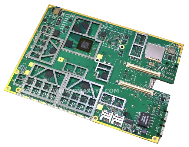
This is a fanless, outdoor-rated Wi-Fi 6 Access Point built around the Qualcomm IPQ8078 SoC, delivering tri-band 802.11ax with 4×4 MU-MIMO across three bands through 12 antennas. It supports LTE/5G, 10G SFP+ fibre, and PoE backhaul, with GPS, BLE, and optional AI/camera expansion on OpenWRT, built for extreme outdoor conditions.
This is a compact, wall-mountable cybersecurity gateway built around the MediaTek MT7986AV SoC, delivering tri-band Wi-Fi 6E with 4×4 MU-MIMO via a fully internal 12-antenna array. It runs OpenWRT with an AI-powered security engine — DNS blocking, reputation filtering, IoT monitoring — backed by 4GB DDR4/32GB eMMC, managed via iOS/Android apps.
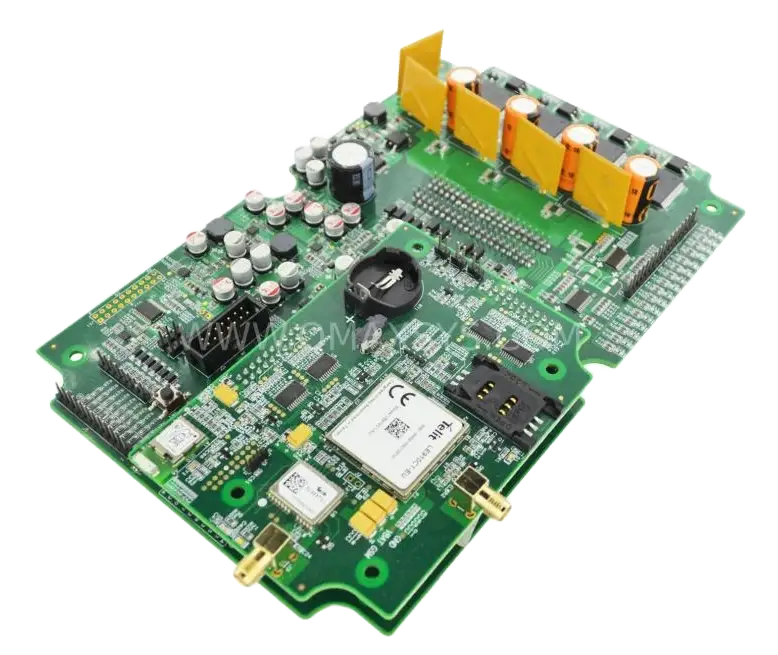
This is a high-performance software-defined radio compute platform built around an Intel NUC8 computing element paired with an Arria 10 FPGA and an AD9375 RF transceiver, interconnected via an embedded controller and Cypress FX3 USB bridge. It integrates Ethernet, mini PCIe, M.2/SATA, GPS, and display interfaces for flexible wireless signal processing.
Click to zoom
1 / 8
EMI, EMC and Pre-Compliance
Why RF Products Fail RE and CE
Radiated emission failures are almost always unintended radiators — an unshielded cable acting as a monopole, a trace that was never bypassed, a slot in an enclosure resonating at a harmonic, a return path that had to detour around a plane split. Conducted emission failures usually trace back to switching converters coupling onto the supply.
Cables and harnesses radiating as unintended antennas
Enclosure seams and apertures resonating at harmonics
Switching-regulator noise conducted onto power lines
Common-mode currents on differential interfaces
What We Do at Design Stage
Compliance is an architecture constraint, not a test event. Analog, high-speed digital, power and RF domains are partitioned before layout, reference planes are kept continuous under every high-speed and RF net, and shielding and filtering are specified rather than added after the first failed scan.
Domain partitioning with star grounding and single-point connections
Board-level shielding cans and chassis-level multi-layer shielding
Tuned Pi-filters at power inputs and snubbers across switching devices
Common-mode chokes selected against measured emission spectra
Ground-loop elimination across analog, digital, power and RF returns
In-House Pre-Compliance
We find and fix emissions in our own lab, before an accredited test house does it at ten times the cost and with a schedule attached. Near-field probing localizes the source to a specific trace, cable or aperture; spectrum analysis quantifies it against the limit line.
Radiated and conducted emission pre-scans against the applicable limit
Near-field probe hunting to localize the offending structure
Rohde & Schwarz CMW500 conformance and EVM measurement
Vector network analysis of matching networks, filters and antennas
Iteration in-house, so the accredited test visit is a confirmation
Regulatory Regimes by Product Class
Getting the regime right matters as much as passing it. A product tested against the wrong part of the rules can pass its scan and still be unsellable. Industrial RF generators are a common trap: a 13.56 MHz plasma generator is not a Part 15 intentional radiator, and treating it as one produces a compliant-looking report against the wrong limit.
Product Class
United States
European Union
India
Intentional radiator — Wi-Fi, BLE, cellular
FCC Part 15 Subpart C
Radio Equipment Directive, EN 300 328 / EN 301 893
WPC ETA; TEC MTCTE where the product is a notified telecom category
Industrial, scientific and medical RF — plasma generators
FCC Part 18 — Class A
EN 55011 / CISPR 11, Group 2 Class A
CISPR 11 as adopted in the Indian Standard series. Outside the WPC ETA regime — industrial RF equipment is not a radiocommunication transmitter
Unintentional radiator — digital host, controller
FCC Part 15 Subpart B
EN 55032 / CISPR 32
BIS registration under the Compulsory Registration Scheme, where the product falls in a notified category
Automotive electronics
—
CISPR 25
AIS-004 (Part 3), the Indian automotive EMC standard, applied alongside CISPR 25
Medical electrical equipment
—
IEC / EN 60601-1-2
CDSCO licensing under the Medical Devices Rules, 2017, with IEC 60601-1-2 as the EMC basis
Immunity, all classes
—
IEC 61000-4 series — ESD, surge, EFT, dips
IEC 61000-4 series, adopted as IS 14700 series
Qmax-designed products have completed formal certification to FCC Part 15 Class A and Class B emissions, FCC Part 18 Class A for industrial RF equipment, SAR for RF human exposure, CE marking, and UL safety listing. Two of those are worth drawing out. Class B is the harder of the two FCC emission classes — the residential limits are tighter than the industrial ones, so a product that clears Class B clears Class A with margin to spare. And SAR is the credential most design houses never acquire, because it only becomes relevant once a transmitter is used close to the body. Passing it means the RF exposure budget was designed in from the antenna placement onward, not discovered at the test house. Qmax Systems works to United States, European Union and Indian regulation, and establishes which regime applies during architecture rather than at the end of the program. Our 13.56 MHz plasma generator is certified as a Class A device under FCC Part 18 — the industrial, scientific and medical rules — not under the Part 15 limits that govern communication radios.
Why Choose Qmax for RF & Microwave Design
Simulation-First RF Engineering
Full-wave 3D electromagnetic simulation runs before the first trace is routed, not after the first board fails. Trace geometry, matching networks, launches, transitions and antenna structures are solved and turned into exact width, gap and length constraints, so the first build meets its VSWR and signal-integrity targets rather than starting an iteration cycle.
Kilowatts and Microvolts in One Team
Most RF houses do high power or high sensitivity. Qmax does both inside one hardware design and development services practice — the engineers who design a kilowatt LDMOS power stage also design the low-noise receive chain and baseband beside it, exactly what a plasma generator or SDR platform needs.
Wireless Coexistence Discipline
Twelve antennas and three concurrent bands in one enclosure is a coexistence problem before it is a throughput problem. We plan frequencies so harmonics and spurs from one radio fall outside another's receive band, then enforce it with high-rejection filtering, deliberate spatial separation and per-section shielding.
In-House RF Validation
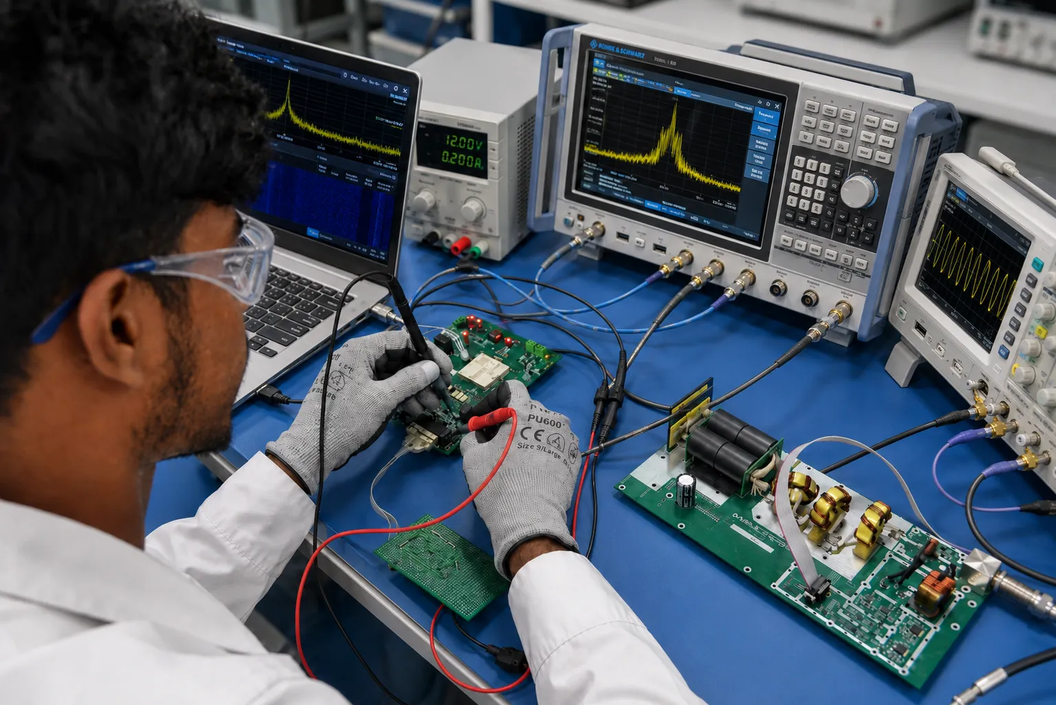
Designs are measured in our own lab on a Rohde & Schwarz CMW500, vector network analyzers, spectrum analyzers and high-bandwidth oscilloscopes. S-parameters, VSWR, EVM, phase noise and emission spectra are verified on real hardware before anything goes to an accredited test house.
Concept to Shipped Product
Our recent plasma generator went from a blank sheet to a shipping product inside Qmax — RF power stage, control loop, shielding, enclosure, compliance and production. That full-lifecycle ownership is why difficult RE and CE problems get solved rather than escalated between vendors who each believe the fault is upstream.
ISO 9001 and ISO 13485 Certified Process
RF problems are expensive to find late and hard to reproduce in the field. Qmax operates ISO 9001 and ISO 13485 certified quality systems, with defined internal process steps and review gates built to catch mistakes before fabrication.
Get a Complimentary Consultation with Our RF & Microwave Experts
A one-hour session with a Qmax Systems Senior Hardware Architect. Bring a link that will not close, an emission you cannot locate, a radio that desenses another, or a matching network that will not hold across the band. Practical and engineering-driven — no sales pitch. We can sign an NDA beforehand.
What frequency and power ranges does Qmax Systems cover?
On frequency, Qmax Systems designs across the full practical RF spectrum — from low-frequency and high-frequency industrial bands, through sub-GHz, the 2.4, 5 and 6 GHz bands and sub-6 GHz cellular, and up to millimeter wave. On power, the range runs from microwatt-class ultra-low-power radios and receive chains recovering signals close to the thermal noise floor, up to kilowatt-class industrial RF generation. Neither range is a limit. The discipline is the same at every point on it — impedance control, matching, isolation, thermal management and electromagnetic containment — so a new band or a new power class is scoped against that engineering, not against a fixed catalog.
How does Qmax Systems handle EMI and EMC in compact designs?
Qmax Systems controls EMI and EMC at the source rather than at the test house. That means partitioning analog, digital, power and RF domains before layout, keeping reference planes continuous beneath every RF and high-speed net, specifying board-level shielding cans and chassis-level shielding as part of the design, and selecting common-mode chokes and Pi-filters against measured emission spectra. Near-field probing then localizes any remaining hotspot to a specific trace, cable or enclosure aperture.
Why do products fail FCC radiated emissions, and how does Qmax Systems prevent it?
Radiated emission failures are usually caused by unintended antennas rather than by the radio itself — an unshielded cable acting as a monopole, a poorly bypassed trace, an enclosure seam resonating at a harmonic, or a return path forced to detour around a plane split. Qmax Systems runs pre-compliance scans in-house with near-field probes and spectrum analyzers to locate the radiating structure, then fixes it with shielding, filtering and bypassing so the design is under limit before formal testing.
What is the difference between pre-compliance and full certification?
Pre-compliance is the engineering phase where EMI and EMC problems are found and corrected, run in-house at low cost and short cycle time. Full certification is the formal testing required for market access, performed by an accredited test house whose report and certificate are the legal artifacts. Qmax Systems runs pre-compliance internally and manages the certification program and the test-house relationship, so the accredited visit confirms a known result rather than discovering a new one. Qmax-designed products have completed certification to FCC Part 15 Class A and Class B, FCC Part 18 Class A, SAR, CE and UL.
How does Qmax Systems prevent desense in multi-radio devices?
Desensitization is designed out through frequency planning first: harmonics and spurious products from one radio must fall outside the receive band of another. That is then enforced physically with high-rejection SAW or BAW filtering, deliberate spatial separation between antennas, per-section shielding cans, and reference-plane discipline. Qmax Systems has applied this on tri-band platforms carrying twelve antennas across three concurrent bands in a single enclosure, including designs with no external antennas at all.
Can Qmax Systems assist with Wi-Fi 6, 6E and Wi-Fi 7?
Yes. Qmax Systems designs Wi-Fi 6, 6E and Wi-Fi 7 hardware including 4×4 and 8×8 MU-MIMO and concurrent tri-band 2.4, 5 and 6 GHz architectures on current Qualcomm and MediaTek platforms. Wi-Fi 7 work involves 320 MHz channels, 4096-QAM and Multi-Link Operation, which raise the bar on phase noise and RF isolation: at 4096-QAM even modest phase noise forces the link down to a lower modulation order, so oscillator and PLL selection becomes a throughput decision.
How does Qmax Systems account for skin effect and copper roughness?
At high frequency current crowds into the surface of the conductor, so the effective resistance rises and the copper profile starts to dominate loss. Qmax Systems specifies foil type — low-profile, very-low-profile or hyper-very-low-profile — alongside surface finish and trace geometry, and applies roughness modeling in simulation rather than assuming a smooth conductor. On high-frequency paths this is the difference between a channel that meets its insertion-loss budget and one that misses it by several dB.
Does Qmax Systems handle mmWave sensor integration?
Yes. Qmax Systems integrates millimeter-wave sensing at 24, 60 and 77 GHz for distance, presence, velocity, level and material measurement, including microwave moisture measurement instruments. At these frequencies trace-width variation of a fraction of a mil produces a measurable impedance discontinuity, so designs use low-loss substrate with tight etch tolerance and full-wave EM extraction of every launch and transition before layout is released.
What in-house RF test capability does Qmax Systems have?
Qmax Systems operates an in-house RF lab equipped with a Rohde & Schwarz CMW500 radio communication tester, vector network analyzers, spectrum analyzers, near-field probes and high-bandwidth oscilloscopes. This supports RF conformance measurement, S-parameter and VSWR characterization, EVM and modulation-quality testing, phase-noise assessment, and radiated and conducted emission pre-compliance scanning — all before a design reaches accredited certification testing.
Can Qmax Systems take over an RF design that is failing compliance?
Yes, and it is a common way our engagements begin. Typical work includes independent review of the schematic, stackup and layout, near-field probing to localize the radiating structure, spectrum measurement against the applicable limit line, and a corrective package covering shielding, filtering, grounding or layout changes. Where the applicable regulatory regime itself was wrong, that is established first — there is no point optimizing against the wrong limit.