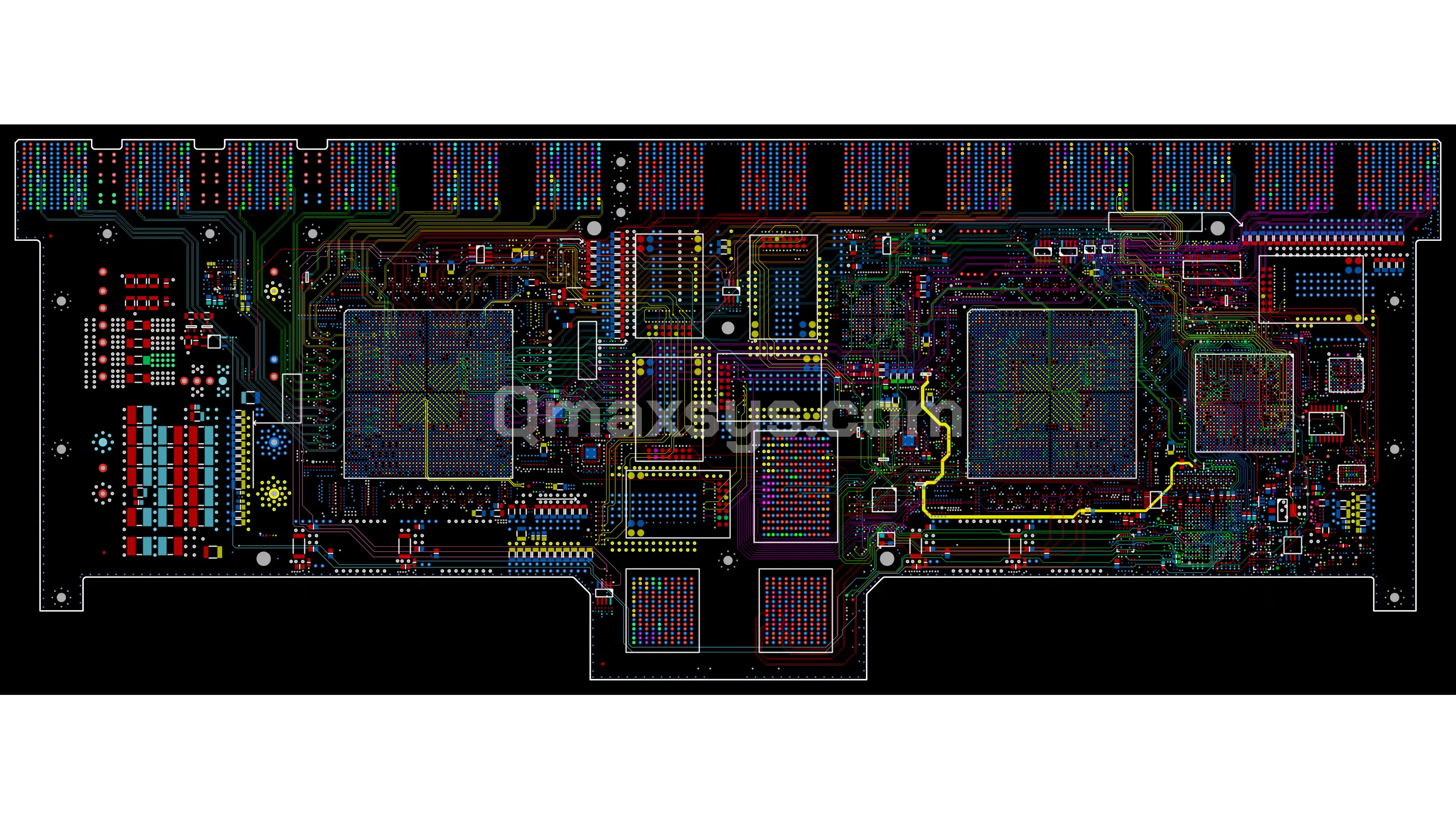
Terabit-Scale Switch Fabric Board
Project Overview
Qmax Systems was engaged by an Indian networking equipment company to execute the full physical PCB design of a terabit-scale switch fabric board built around dual Broadcom BCM88750 (FE1600) fabric elements. The customer supplied verified schematics and a design-input package; Qmax owned the layout of a 30-layer, controlled-impedance, carrier-grade backplane fabric card. The board switches cell-based traffic between up to 14 line-card slots across a chassis midplane, making high-speed SerDes routing, power integrity, and manufacturability the central engineering challenges. Qmax delivered a fabrication-ready design closing on signal integrity, PDN, and DFM targets for a regulated telecom-class product.
Application Brief
The board is the central switch fabric card inside a modular, chassis-based packet-optical transport platform used by service providers for metro and core Carrier Ethernet / MPLS aggregation. Two BCM88750 (FE1600) fabric elements — each rated at 1.6 Tbps of full-duplex switching capacity, giving up to ~3.2 Tbps of aggregate installed fabric bandwidth on a single board — form a non-blocking, self-routing switching mesh that interconnects up to 14 line-card slots over the chassis backplane. The platform runs on redundant -48 V DC telecom power, carries IPMC-based shelf management for hot-swap operation, and distributes precision network timing (IRIG / BITS-class reference). At the PCB level this terabit-scale throughput translates into 96 matched high-speed SerDes links, deep power/ground plane segmentation, and full hot-swap and manageability support — all on a single controlled-impedance card.
Qmax Scope
Qmax Systems owned the full PCB design of the switch fabric card, from design-input review through fabrication data release:
- Design-input review — captured customer schematics, mechanical outline, BoM, net classes, and electrical constraints (HV, high-current, high-speed digital, analog, and mixed-signal domains)
- 30-layer stackup design — defined a controlled-impedance stackup with 14 routing layers and 16 power/ground planes at 127 mil finished thickness
- High-speed SerDes routing — routed 96 fabric SerDes differential pairs (48 RX + 48 TX ARAD links) plus the 14-slot backplane fabric buses with strict impedance and skew control
- Dual-fabric placement — floor-planned both BCM88750 BGA devices and their far-side backplane connectors to equalise lane lengths to all line-card slots
- Power delivery network design — planned multi-rail PDN spanning -48 V input, 12 V intermediate, and sub-1 V core rails with sensed core supplies and isolated analog rails
- Signal integrity review — impedance, insertion/return-loss, crosstalk, and skew verification for all fabric SerDes and backplane channels
- Power integrity review — PDN impedance targeting and decoupling strategy across the segmented plane structure feeding the fabric BGAs
- Backplane connector escape — designed the high-density Molex Fabric Farside and Impact mezzanine escape routing under fine-pitch fields
- Manageability & timing routing — laid out I²C/SMBus, JTAG, MDIO, UART, and IPMC control nets plus precision clock and IRIG timing distribution
- DFM and fabrication release — DFM review against fab and assembly constraints, drill/padstack audit, and full Gerber / fabrication data package release
Challenges & Resolutions
Dual 2,397-Ball Fabric BGA Breakout
Each BCM88750 required a multi-layer escape; Qmax used a structured via-and-plane escape across inner signal layers to release all SerDes without starving top-layer routing.
96 Length- and Skew-Matched SerDes Pairs
Intra-pair, intra-lane, and lane-to-lane matching was applied across 48 RX and 48 TX ARAD differential pairs to preserve eye margin at fabric line rates.
Equalising 14 Backplane Slot Links
Central placement of the two fabric devices balanced trace lengths from the switch cores to all 14 far-side backplane connectors, minimising slot-to-slot skew.
Dense Plane Segmentation on 30 Layers
16 power/ground planes were partitioned to give every high-speed layer a continuous adjacent reference while isolating the four sensed 1V0 analog fabric rails.
High Through-Via Count Management
Over 10,300 through-vias were planned with disciplined via-field and antipad strategy to protect impedance and keep routing channels open.
-48 V Telecom Power Integrity
Redundant fused -48 V feeds and hot-swap-capable conversion were laid out with wide, low-impedance copper and careful creepage/clearance for the high-voltage input section.
Isolated Analog Fabric Supplies
Four separate 1V0 analog rails (per fabric quadrant) were routed with sensed feedback and local decoupling to protect SerDes PLL performance from digital-rail noise.
Precision Timing Distribution
Low-jitter reference clocks and IRIG-A/B timing nets were routed with guarding and matched lengths, kept clear of noisy switching and power regions.
Hot-Swap / IPMC Manageability
The SmartFusion-based IPMC domain, I²C/SMBus trees, and standby rails were laid out to support live insertion/removal without disturbing the active fabric.
Carrier-Grade DFM Closure
The layout was reviewed against fabrication and EMS constraints (drill sizes, aspect ratio, connector press-fit, padstacks) to release manufacturing data without a re-spin.
Major HW Components
Dual Broadcom BCM88750 (FE1600)
2,397-ball fabric element devices forming the redundant, non-blocking switching mesh (U1, U2)
IDT 89HPES16NT16G2
16-lane PCIe Gen2 non-transparent switch routing the control plane between the local processor and fabric domain
Microsemi A2F200M3F SmartFusion
FPGA + Cortex-M3 device serving as the Intelligent Platform Management Controller (IPMC) for hot-swap and health monitoring
Altera EP2AGX95 Arria II GX FPGA
High-speed SerDes-capable FPGA handling fabric-side glue logic and control interfacing
Silicon Labs Si5374 / Si530 / Si5330
Jitter attenuator and low-jitter clock generators/oscillators for network synchronisation
Ericsson BMR462 / BMR464 / PIM4000
Digital point-of-load and intermediate-bus power modules for the multi-rail PDN
Molex Fabric Farside Connectors (J1–J14)
High-density backplane connectors carrying the 14-slot fabric SerDes to the chassis midplane
Molex Impact Mezzanine Headers (J25–J27)
High-speed mezzanine interfaces for the control/management daughter interface
Atmel AT24Cxx / AT25DF321 / EPCS128
Board-ID EEPROMs and configuration flash for FPGA boot and FRU data
LM84 / DS75 Thermal Sensors & LTC4300/LTC4313
Temperature monitoring and I²C bus buffering for the shelf-management subsystem
Major Interfaces
Fabric SerDes Links
96 high-speed differential pairs (48 RX + 48 TX ARAD channels) between the fabric elements and line-card connectors
14-Slot Backplane Fabric Buses
NODE1–NODE14 multi-lane differential buses to the chassis midplane, one bus per line-card slot
PCIe Gen2 (Control Plane)
16-lane non-transparent PCIe fabric via the IDT switch linking the local processor to the management domain
I²C / SMBus
Multi-segment management topology with bus buffers and multiplexers across the shelf-management subsystem
JTAG
Boundary-scan and configuration chains across the fabric BGAs, FPGAs, and CPLDs
MDIO
Management data interface for PHY/SerDes-side control
UART / RS-232
Console and inter-processor serial links for the control and management processors
SPI
Configuration-flash and peripheral interface for FPGA boot and device setup
Precision Timing (IRIG-A/B, BP_REF_CLK)
Backplane reference-clock and IRIG timecode distribution for network synchronisation
Redundant -48 V DC Power
Dual fused -48 V telecom feeds with 12 V intermediate bus and sub-1 V core rails
PCB Design Specifications
Summary
Qmax Systems delivered a complete, fabrication-ready layout of a 30-layer, terabit-scale switch fabric card built on dual Broadcom BCM88750 (FE1600) fabric elements, carrying up to ~3.2 Tbps of aggregate installed switching bandwidth. The design closed on signal integrity, power integrity, and DFM targets across 96 matched SerDes pairs, a 14-slot backplane, deep plane segmentation, and carrier-grade -48 V power — from customer design inputs through to Gerber release. The project demonstrates Qmax's capability to take on the most demanding high-speed, high-layer-count telecom fabric designs and drive them to manufacturing without a re-spin.